

Ion beam irradiating apparatus, and method of producing semiconductor device
a technology of ion beam and irradiation apparatus, which is applied in the field of ion beam irradiation apparatus and method of producing semiconductor devices, can solve the problems of difficult to efficiently neutralize the space charge of the ion beam, and achieve the effect of efficient neutralization, improved transport efficiency of the ion beam, and improved efficiency
- Summary
- Abstract
- Description
- Claims
- Application Information
AI Technical Summary
Benefits of technology
Problems solved by technology
Method used
Image

Examples
Embodiment Construction
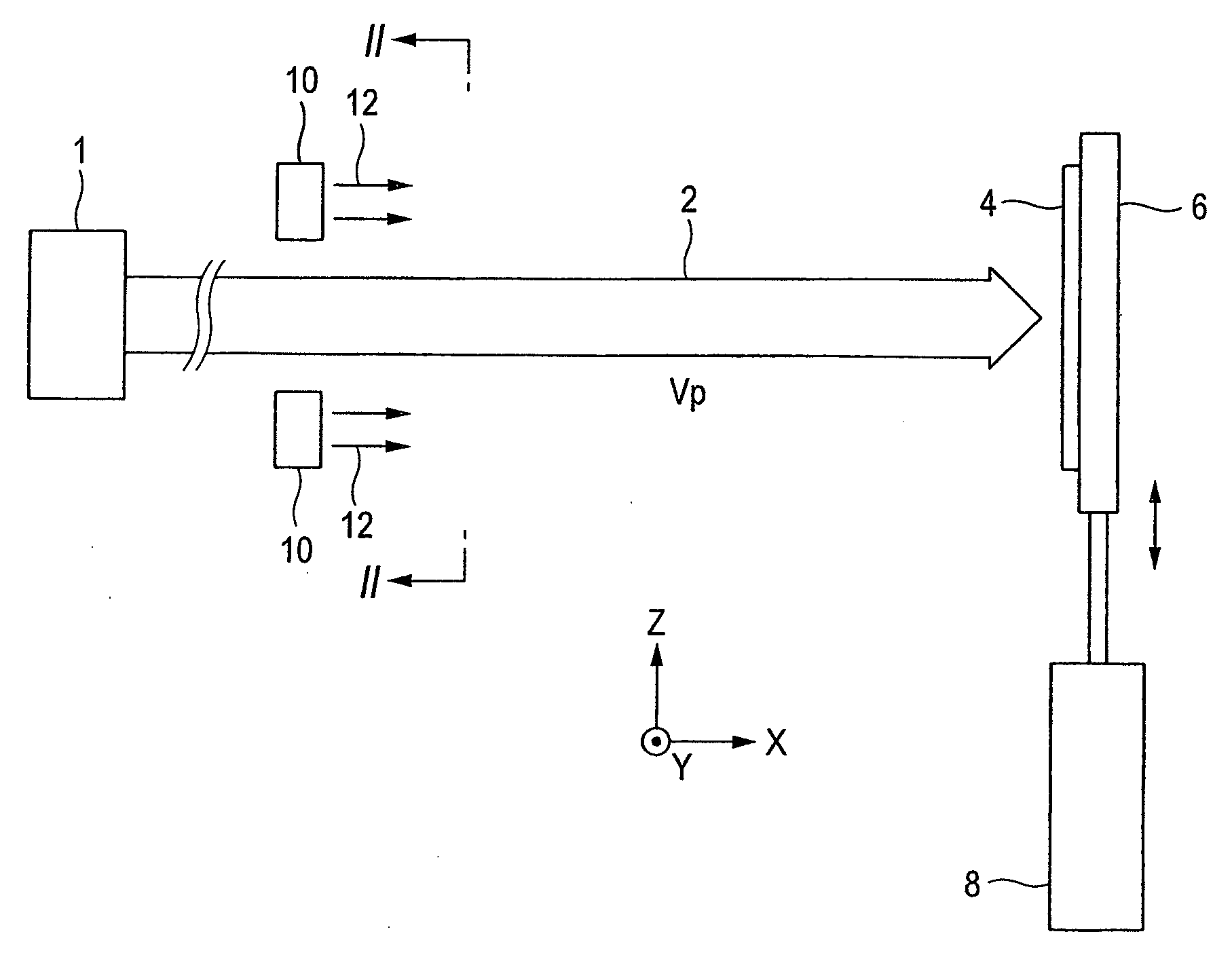
[0049]FIG. 1 is a schematic side view showing an embodiment of the ion beam irradiating apparatus of the invention. The ion beam irradiating apparatus is configured so that a target 4 held by a holder 6 is irradiated with an ion beam 2 extracted from an ion source 1 to perform a process such as ion implantation on the target 4. The holder 6 is at, for example, the ground potential. The transporting path of the ion beam 2, and the holder 6 are placed in a vacuum chamber which is not shown, to be in a vacuum atmosphere. For example, the target 4 is a semiconductor substrate, a glass substrate, or the like.
[0050]In the transporting path of the ion beam 2 extending from the ion source 1 to the holder 6, as required, a mass separator which separates the mass of the ion beam 2, a scanner which performs a scanning operation on the ion beam 2, and the like are disposed.
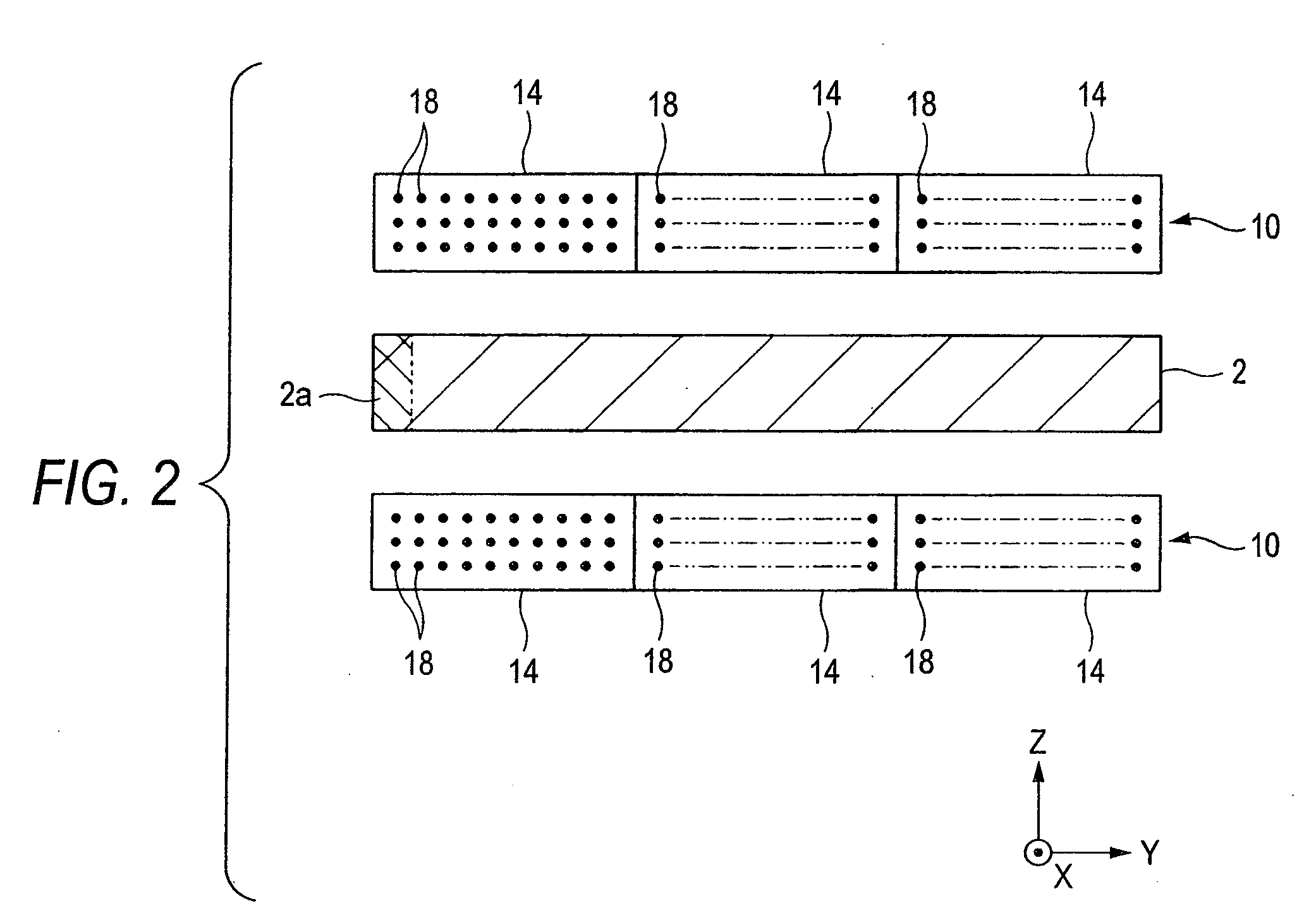
[0051]Field emission electron sources 10 which emit electrons 12 are disposed in the vicinity of the path of the ion beam 2...
PUM
 Abstract
Description
Claims
Application Information