

Acoustic wave device physical parameter sensor
a technology of acoustic wave and a sensor body, applied in the field of parameter sensing, can solve the problems of poor accuracy or expensive correction measures, sensors that cannot support high sensitivity, and disadvantages in size, price, power, data output access, etc., and achieve low price, low power operating range, and small size
- Summary
- Abstract
- Description
- Claims
- Application Information
AI Technical Summary
Benefits of technology
Problems solved by technology
Method used
Image

Examples
embodiment 100
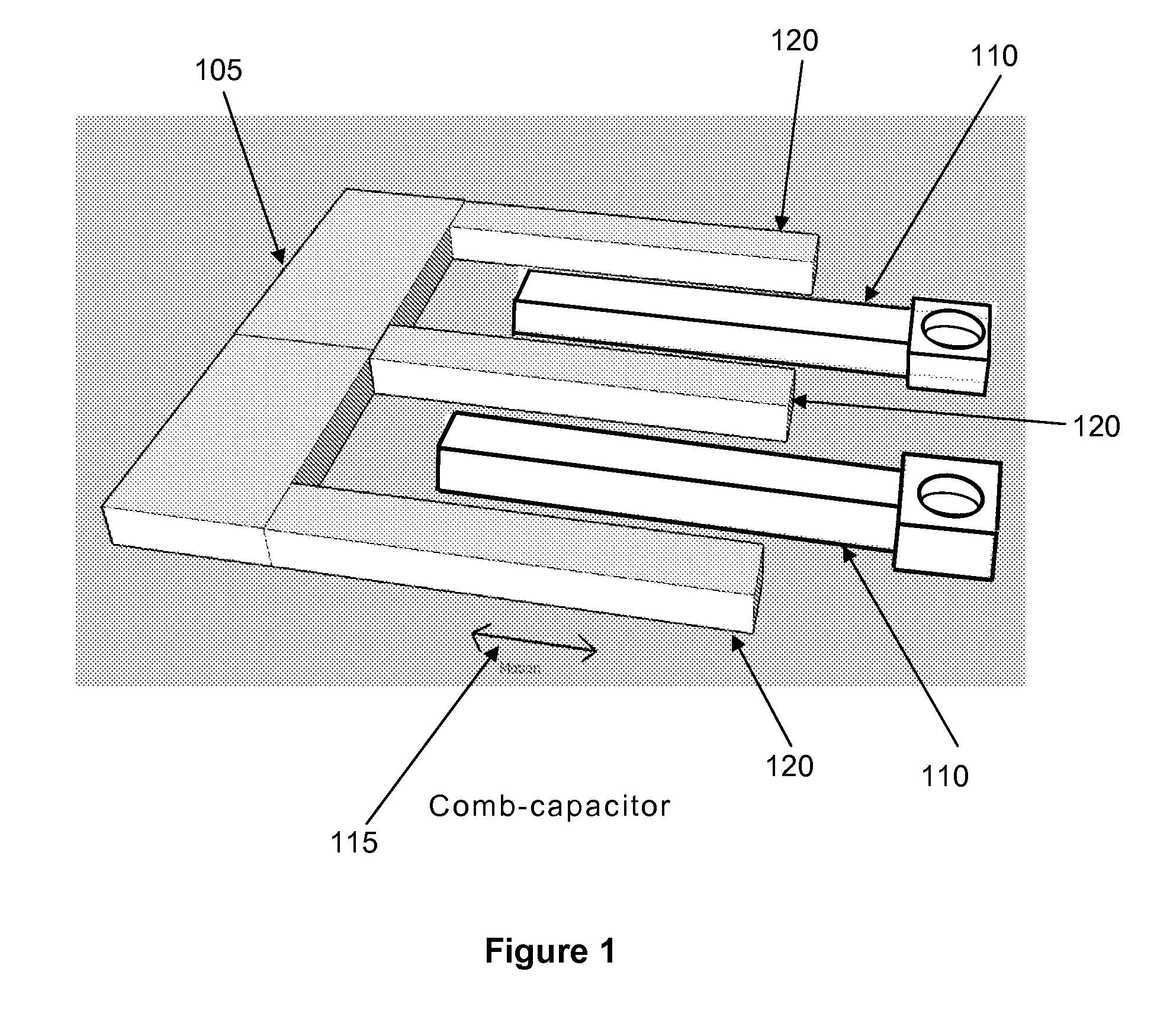
[0062]In FIG. 1, a comb capacitor Micro-Electro-Mechanical-system (MEMS) embodiment 100 is used to realize the load capacitor. Both the comb as well as cantilever and bridge embodiment structures can be used to realize the load capacitor values. Advantages of using MEMS structures include low price and size and the ability to incorporate the structure on an integrated circuit.
[0063]Note that SAW modeling allows one to calculate the capacitance of a comb structure since a similar structure is used in SAW interdigital transducers; this does not mean that only SAW-type sensors are used. It means that the absolute value of the external capacitor in this embodiment can be determined by using simple SAW inter-digital transducer (IDT) analytical expressions or computer aided design methods, or it can be physically measured. This capacitance value is then correlated to the sensed parameter value. Simulation results of an external capacitor in parallel connection with a one port resonator, a...
embodiment 200
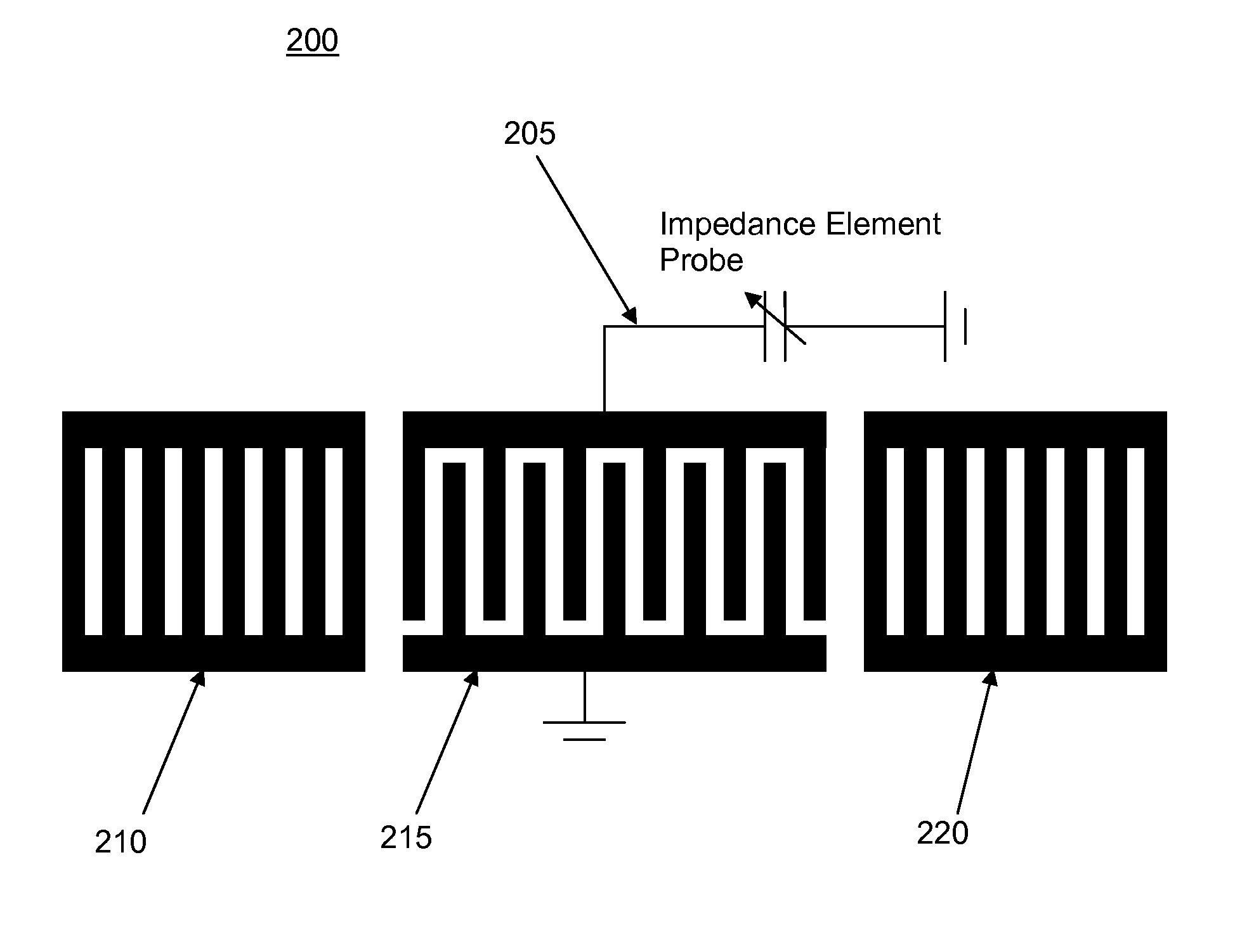
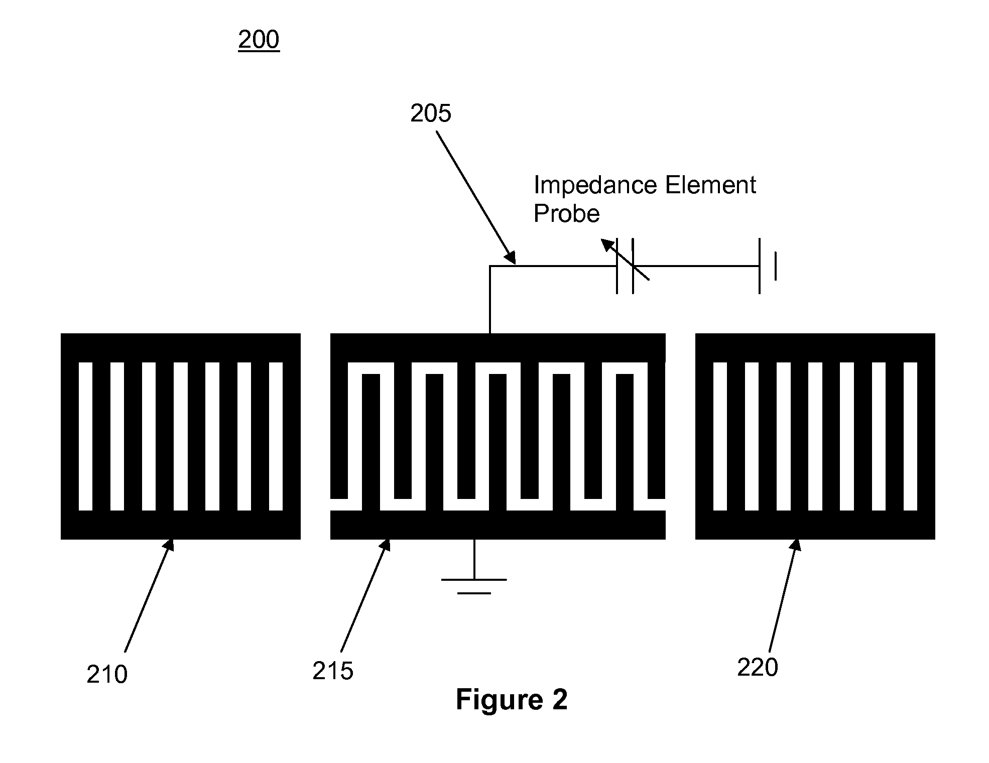
[0065]FIG. 2 illustrates an embodiment 200 having an operable connection between a surface acoustic wave one port resonator 215 with external impedance element probe 205. Note that the component indicated by the variable capacitor symbol 205 is illustrative only and any two-terminal impedance element or network may be employed. Other figures include a variable impedance symbol. The variable impedance symbol is meant to include variable capacitors. As previously stated, note also that operably coupled or connected includes inductively and capacitively coupled elements and that a direct conductive connection is not required. This configuration with reflectors 210, 220 maximizes sensitivity but may incur a variation of the input matching conditions. Therefore, in some applications, it may be desirable to employ a “two port” sensing element as in FIGS. 3A and 3B.
[0066]FIG. 3A displays an embodiment 300A with a connection between a surface acoustic wave two port resonator IDT 315 and ref...
embodiment 400
[0068]FIG. 4 displays an embodiment 400 with a transmission based sensor (e.g. a feedback oscillator circuit) using a three IDT device consisting of an input port 405, an output port 410, a sensing port 415, plus reflectors 420 and 425. Operable connections are between an IDT (sensing port) and external impedance element probe 430. Again, any two terminal impedance element or network may be employed. Also, the arrangements of inputs, outputs, and sensing ports may be varied and more arrangements can be employed in other embodiments for specific delay line and resonator geometries including the use of a plurality of sensing ports.
PUM
 Abstract
Description
Claims
Application Information