Resonant MEMS device that detects photons, particles and small forces

a mems device and photon technology, applied in the field of microelectromechanical systems, can solve the problems of reducing switching reliability, unable to detect extremely small deflection angles, and affecting the reliability of mems switches

Inactive Publication Date: 2009-08-20
SCANNANOTEK
View PDF5 Cites 17 Cited by
  • Summary
  • Abstract
  • Description
  • Claims
  • Application Information

AI Technical Summary

Benefits of technology

[0013]A method of producing the resonant MEMS device of the invention creates an insulation layer on top of a substrate and dispose at least one sensor electrode on the insulation layer. The method further couples a transition layer having a width in the range of 0.5 Å to 100 Å to the sense electrode and couples a micro-mechanical structure that resonates at an oscillation amplitude and an oscillation freq...

Problems solved by technology

In situations where two surfaces scaled in the micrometer ranges come into close proximity, such surfaces may adhere to each other because, at such small scale, electrostatic (and/or Van der Waals) forces become significant producing a problematic phenomena known as stiction.
MEMS switches suffer from stiction when the different electrical potentials applied to the electrodes reduces switching relia...

Method used


Image

  • Resonant MEMS device that detects photons, particles and small forces
  • Resonant MEMS device that detects photons, particles and small forces
  • Resonant MEMS device that detects photons, particles and small forces

Examples


Embodiment Construction

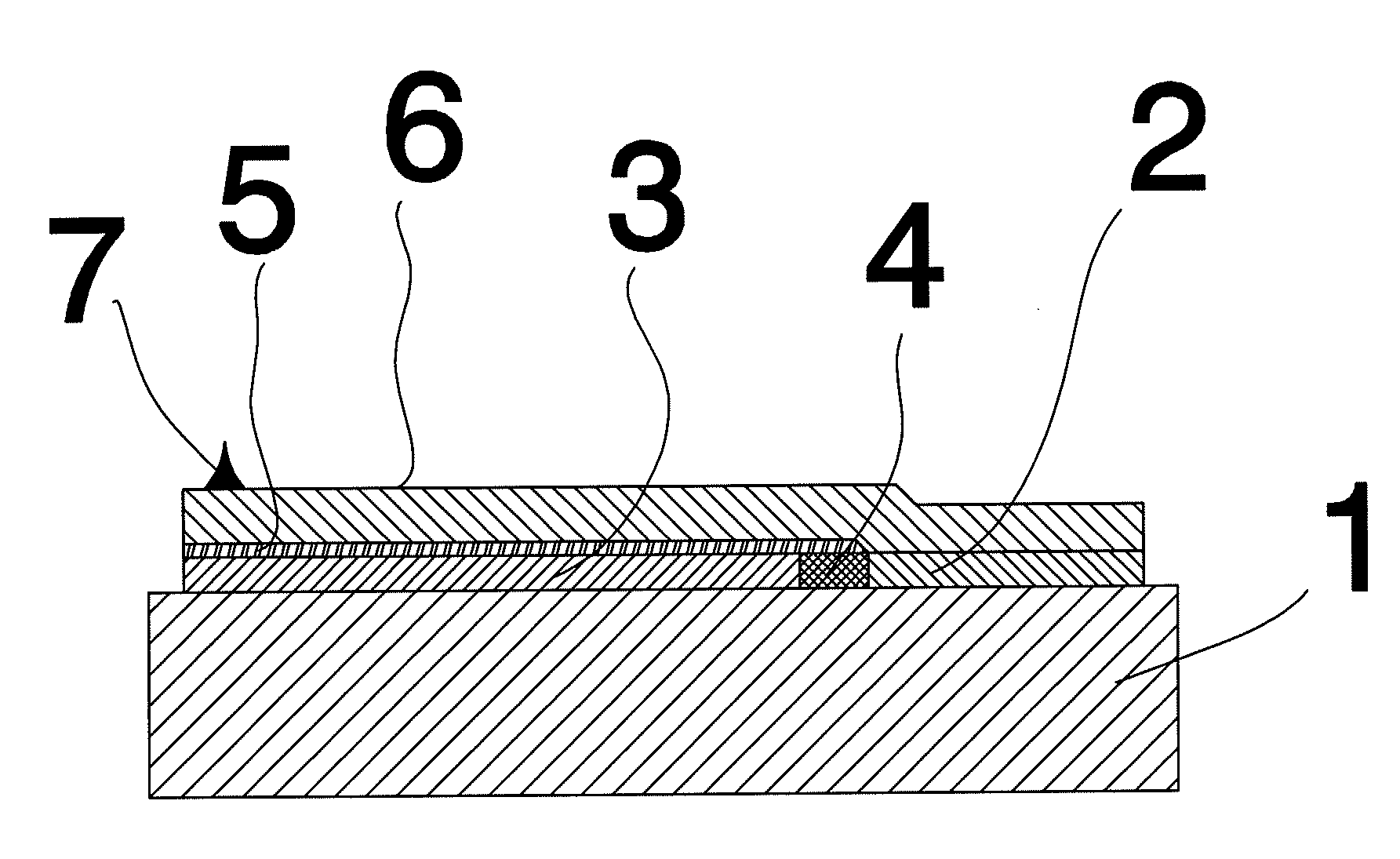
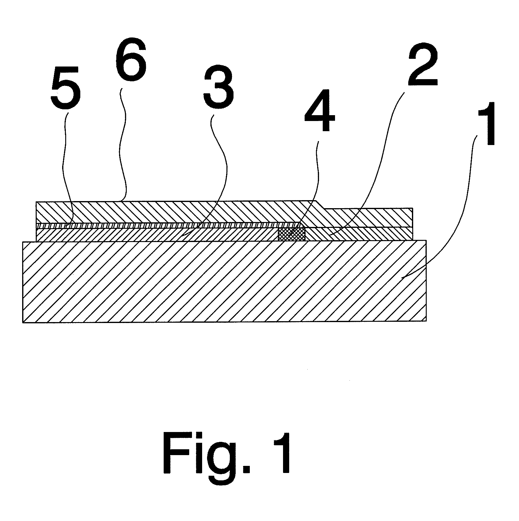
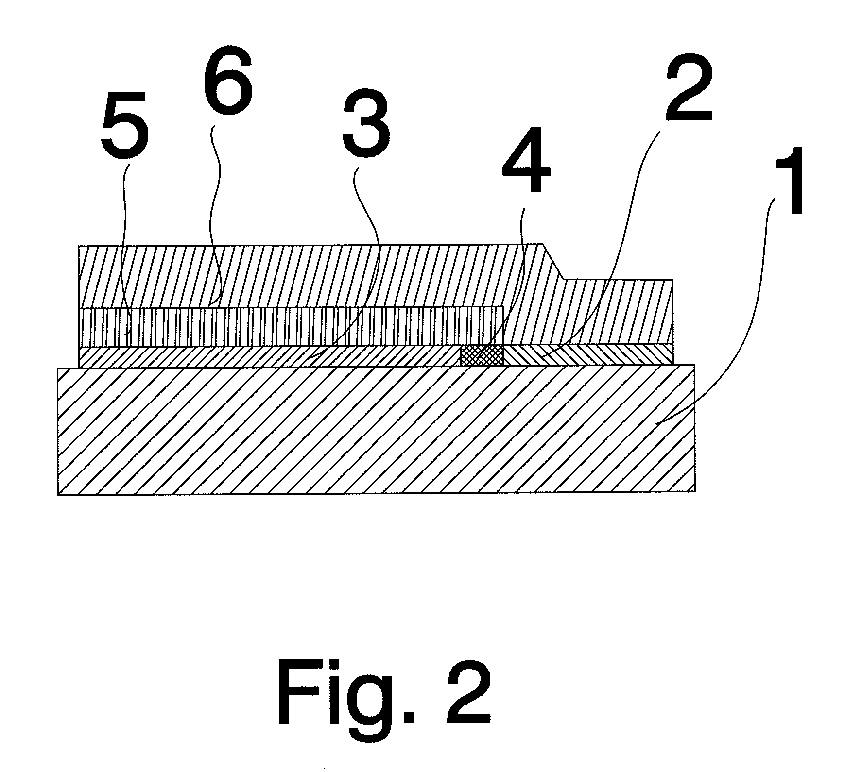
[0026]The resonant MEMS device according to the present invention includes a micro-mechanical structure disposed on a substrate via a resonator electrode that is electrically insulated from a sensor electrode. A thin transition medium having a thickness in the range of 0.5 Ångstrom (Å) to 100 Ångstrom (Å), made of suitable material is disposed between the sensor electrode and the micro-mechanical structure within a relatively small gap, herein after called a nano-gap in the range of 0.5 angstrom (Å) to 100 angstrom (Å). The micro-mechanical structure is designed to have a relatively small maximum oscillation amplitude at its natural frequency as defined by the material and geometry of the micro-mechanical structure and / or the transmission medium. The maximum oscillation amplitude is coupled to the transmission medium to enable flow of tunnelling electrons in such a way that any relative change in oscillation amplitude due to an external force corresponds to one or more properties as...


PUM


Abstract

A resonant MEMS device that detects photons, particles and small forces including atomic forces is disclosed. The device comprises a planar substrate 1, two electrodes 2 and 3 on top of the substrate, a resonant micro-electromechanical (MEMS) structure 6, such as a cantilever, anchored to first electrode 2 and arranged above the second electrode 3 separated from this electrode with an ultrathin transition layer 5. The resonant MEMS structure is working at its natural resonant frequency. The resonant oscillation of the cantilever can be initiated by applying AC voltage with frequency equaling the resonant frequency of the MEMS structure. A constant voltage is applied between the cantilever and the second electrode. The cantilever oscillates at very small amplitude ranging from few Ångstrom (Å) to several nm. During operation, a constant component of the electrical current is measured between the cantilever and the second electrode 3. The electrical current is a tunnelling current described by quantum mechanical probability with which the electrons can tunnel through the transition layer. The thickness of the transition layer is selected so that at no resonance the constant component of the electrical current is about zero and at resonance the DC electrical current has non-zero value and reaches its maximum. When the cantilever interacts with photons, particles or atoms on surfaces then the MEMS device measures their energies using change in the DC tunnelling current and shift of resonant frequency.

Description

CROSS-REFERENCE TO RELATED APPLICATIONS[0001]This Non-provisional Application claims the benefit of U.S. Provisional Application Ser. No. 61 / 064,084, filed Feb. 15, 2008, which is incorporated by reference herein in its entirety.FIELD OF THE INVENTION[0002]The present invention relates to micro-electromechanical systems (MEMS) and, more particularly, to MEMS devices having a resonating micro-mechanical structure that induces tunnelling effect current for detection of very small particles, elementary particles, photons and very small forces.BACKGROUND OF THE INVENTION[0003]MEMS are devices having sub-millimeter-sized micro-mechanical components. Some MEMS have a resonating micro-mechanical structure that oscillates at its natural frequency. Resonator MEMS have been used in switches (U.S. Pat. No. 6,744,338 B2) and tunable capacitor application (U.S. Pat. No. 7,095,295 B1). The resonating micro-mechanical structures in these devices comprises a cantilever that resonates within a relat...

Claims


Application Information

Patent Timeline
IPC IPC(8): H03H9/46
CPCB82Y35/00H03B5/30G01Q20/04G01J1/42
Inventor PAVLOV, ANDREIPAVOLVA, YELENA
Owner SCANNANOTEK
Why Eureka
Try Eureka