
Decoupling capacitors

a capacitor and capacitor electrode technology, applied in the direction of fixed capacitor electrodes, basic electric elements, electric devices, etc., to achieve the effect of low leakage, high capacitance, and small area

Active Publication Date: 2009-08-20
ARM LTD
View PDF4 Cites 16 Cited by
  • Summary
  • Abstract
  • Description
  • Claims
  • Application Information

AI Technical Summary

Benefits of technology

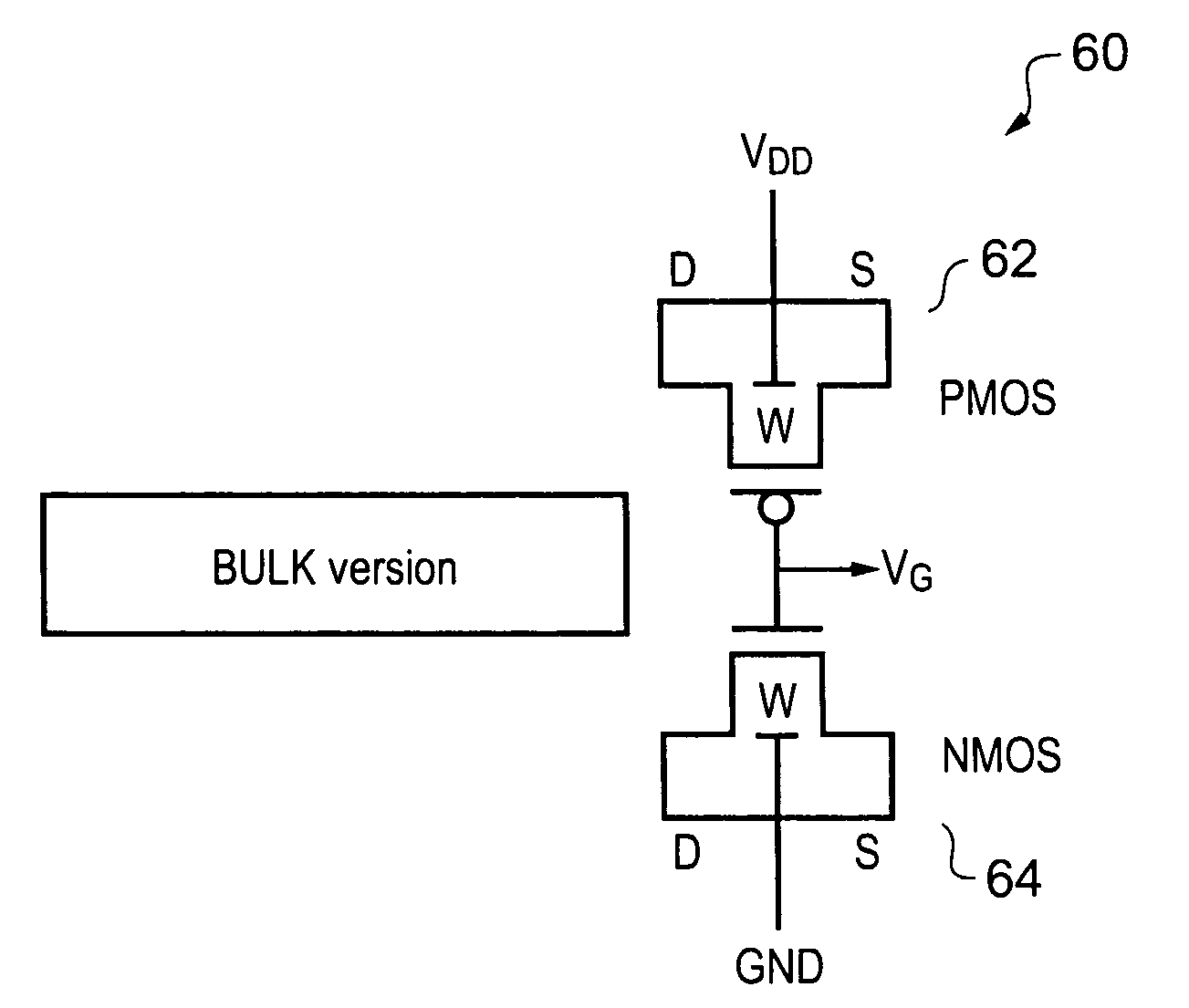
[0011]The formation of a decoupling capacitor from two transistors a p-type and an n-type provides an advantage of increased capacitance compared to a single transistor capacitor and an additional advantage that two transistors can be formed in a relatively small area such that the capacitance density is high. Furthermore, as there is a device of each type then the boundary between the n-type and p-type portions can be straight as the use of two devices of opposite types means that there is no, or at least a reduced advantage, to be gained by increasing the area of one of the type portions with respect to the other by for example, well jogging. Well jogging is to be avoided if possible as it increases the well proximity to other adjacent devices which can cause problems particularly with small devices in close proximity to each other.
[0040]A decoupling capacitor can also be formed from two reverse bias diodes. These have the advantage of a small area, high capacitance, low leakage and the same well / substrate structure as other standard cells.

Problems solved by technology

Well jogging is to be avoided if possible as it increases the well proximity to other adjacent devices which can cause problems particularly with small devices in close proximity to each other.

Method used


Image

  • Decoupling capacitors
  • Decoupling capacitors
  • Decoupling capacitors

Examples


Embodiment Construction

[0055]FIG. 3a shows a decoupling capacitance according to an embodiment of the present invention. It comprises an NFET transistor 30 arranged in parallel with a PFET transistor 40. As can be seen by the layout diagram FIG. 3b, which shows two of the structures adjacent to each other this is a symmetrical structure which therefore enables the boundary between the nwell and the p type substrate to be straight and also results in there being very little unused space on the silicon. Thus, the capacitance density of this structure is high.

[0056]In this embodiment, the gates of the FET's are attached to the supply nodes through a diffusion layer 50. This is referred to as a diffusion jumper and is used to increase the amount of series resistance. In some embodiments, where series resistance is not required then these gates can be connected to the supply nodes using a metallisation layer.

[0057]As can be seen with this layout the decoupling capacitance density is primarily limited by the ma...


PUM


Abstract

A decoupling capacitor is disclosed that has an n-type portion and a p-type portion in a semiconductor, said decoupling capacitor comprising an NFET transistor and a PFET transistor, said PFET transistor being substantially formed in said n-type portion and said NFET transistor being substantially formed in said p-type portion, a boundary between said n-type portion and said p-type portion being substantially straight, said transistors being arranged such that a source and drain of said PFET transistor are connected to a high voltage rail and a source and drain of said NFET transistor are connected to a low voltage rail.

Description

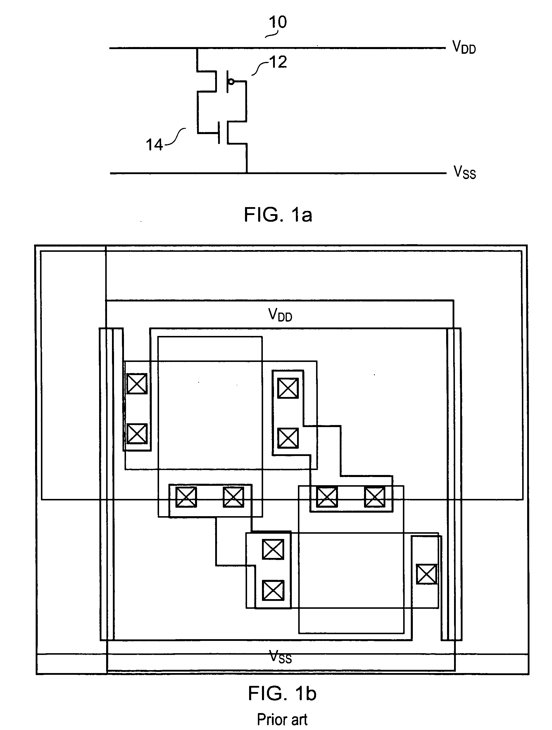
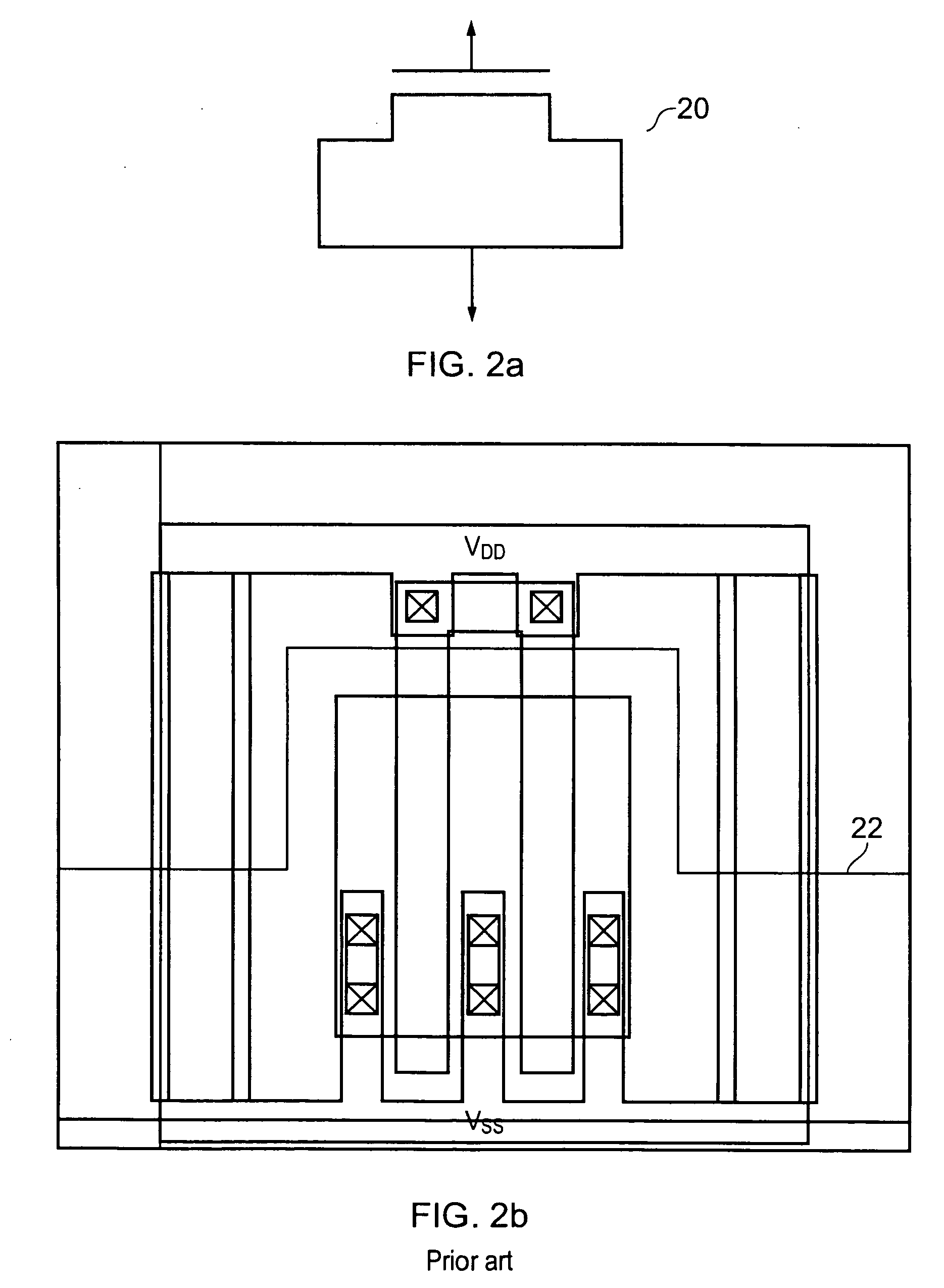
BACKGROUND OF THE INVENTION[0001]1. Field of the Invention[0002]The field of the invention relates to decoupling capacitors for decoupling one part of an electrical circuit from another.[0003]2. Description of the Prior Art[0004]Decoupling capacitors are often used in modern powered circuits. They are used, for example, to compensate for fluctuations in the power supplied to a circuit. These fluctuations can be caused by AC signals superimposed on a DC power line or by switching in another circuit located close to the circuit in question. Decoupling capacitors are also be used to compensate for dips in the power supply due to circuits pulling load from the power supply.[0005]Decoupling capacitors are generally arranged in parallel with the circuits that they are providing fluctuation compensation for. Arranged in this way they charge up when the power supply is high and discharge to compensate for dips when the voltage level drops.[0006]FIG. 1a shows in circuit form and FIG. 1b in l...

Claims


Application Information

Patent Timeline
IPC IPC(8): H01G4/35
CPCH01G4/35
Inventor FREDERICK, JR., MARLINCLARK, DAVID PAULPELLOIE, JEAN-LUCCHONG, YEW KEONG
Owner ARM LTD
Learn More