

Semiconductor device
- Summary
- Abstract
- Description
- Claims
- Application Information
AI Technical Summary
Benefits of technology
Problems solved by technology
Method used
Image

Examples
Embodiment Construction
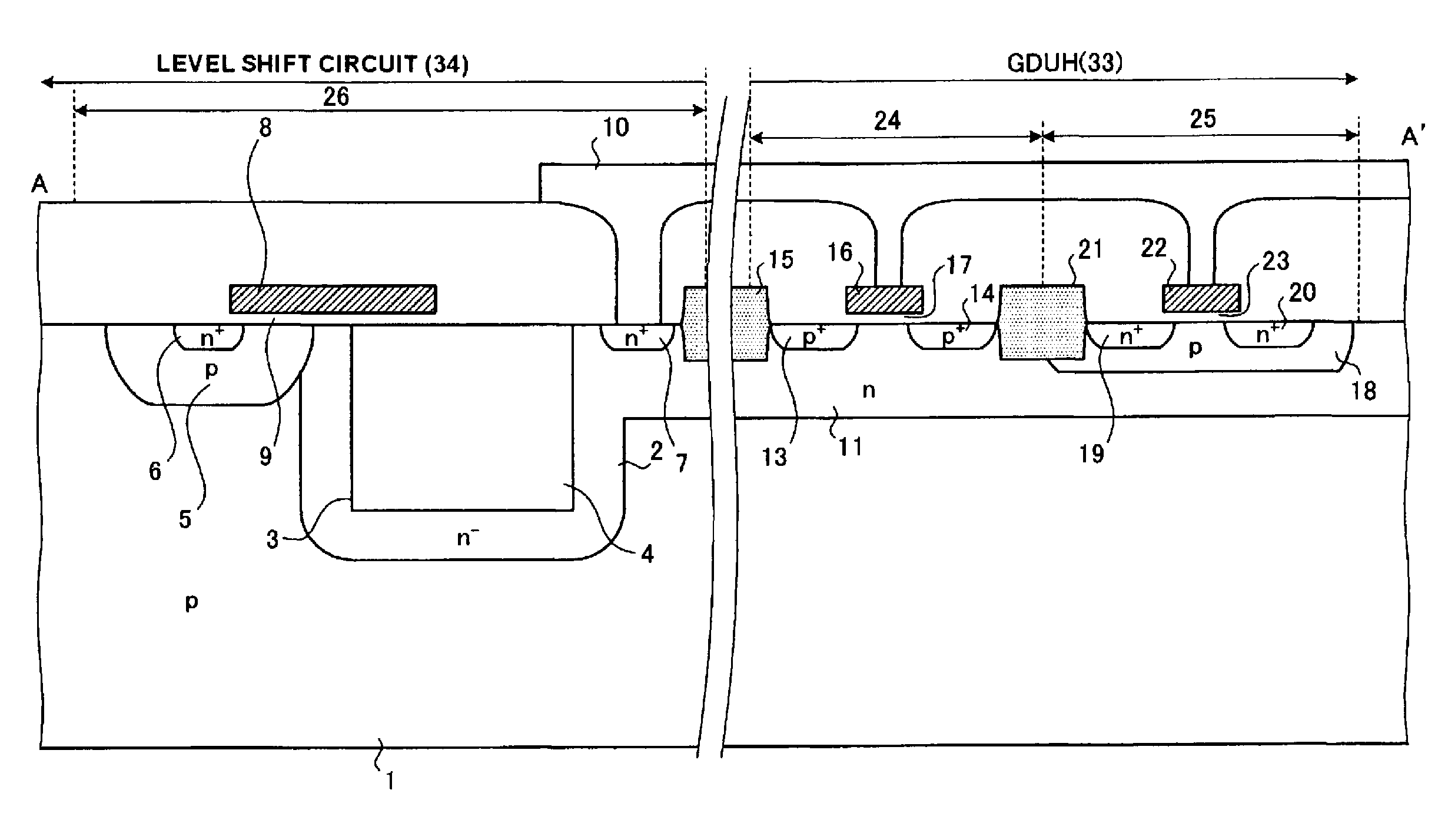
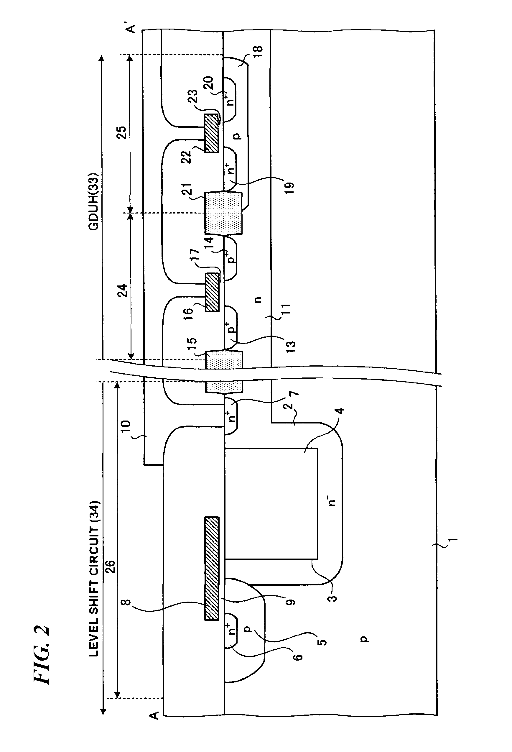
[0042]FIG. 1 is a top plan view of a semiconductor device according to the invention. The semiconductor device shown inFIG. 1 is employed for a high-potential gate driver circuit (hereinafter referred to as “GDUH”) 33 of a controller used for inverters that provide illumination. The semiconductor device according to the invention shown in FIG. 1 is formed in an island separated electrically from low-potential gate driver circuit (hereinafter referred to as “GDUL”) 32 by a junction separation structure or a dielectric separation structure, and the peripheral portion thereof is surrounded by a high-breakdown-voltage junction edge-termination structure (hereinafter referred to simply as “edge termination structure”) 36. In the semiconductor device, a lateral MIS transistor, which exhibits a high-breakdown voltage and works for level shift circuit 34, is disposed. The lateral MIS transistor includes p-type base layer 5, n+-type source layer 6, n+-type drain layer 7, and gate electrode 8...
PUM
 Abstract
Description
Claims
Application Information