
Electronic component and method of manufacturing the same

a technology of electronic components and manufacturing methods, applied in the field of electronic components, can solve the problems of inability to secure the insulation between bumps, i.e. between terminals, and achieve the effect of reducing resistance values and shortening feed lines

Inactive Publication Date: 2009-08-27
TAIYO YUDEN KK
View PDF6 Cites 15 Cited by
  • Summary
  • Abstract
  • Description
  • Claims
  • Application Information

AI Technical Summary

Benefits of technology

[0034]By means of this aspect, opposing first terminal electrodes can be connected over the shortest distance on the substrate prior to cutting. Hence the feed line resistance can be reduced.
[0039]According to the fourth aspect, there is no uncut feed line remaining along edges of the substrate, so that the yield of electronic components with terminals formed thickly by plating can be improved.
[0056]By means of this aspect, in the process to cut the substrate, identification of the region for cutting (the intended cutting region) is made easy, so that electronic component productivity is improved.
[0059]By means of this aspect, in the process of cutting the substrate, substrate chipping can be prevented.
[0062]By means of this aspect, in the process of cutting the substrate, identification of the dicing lines is made easy.
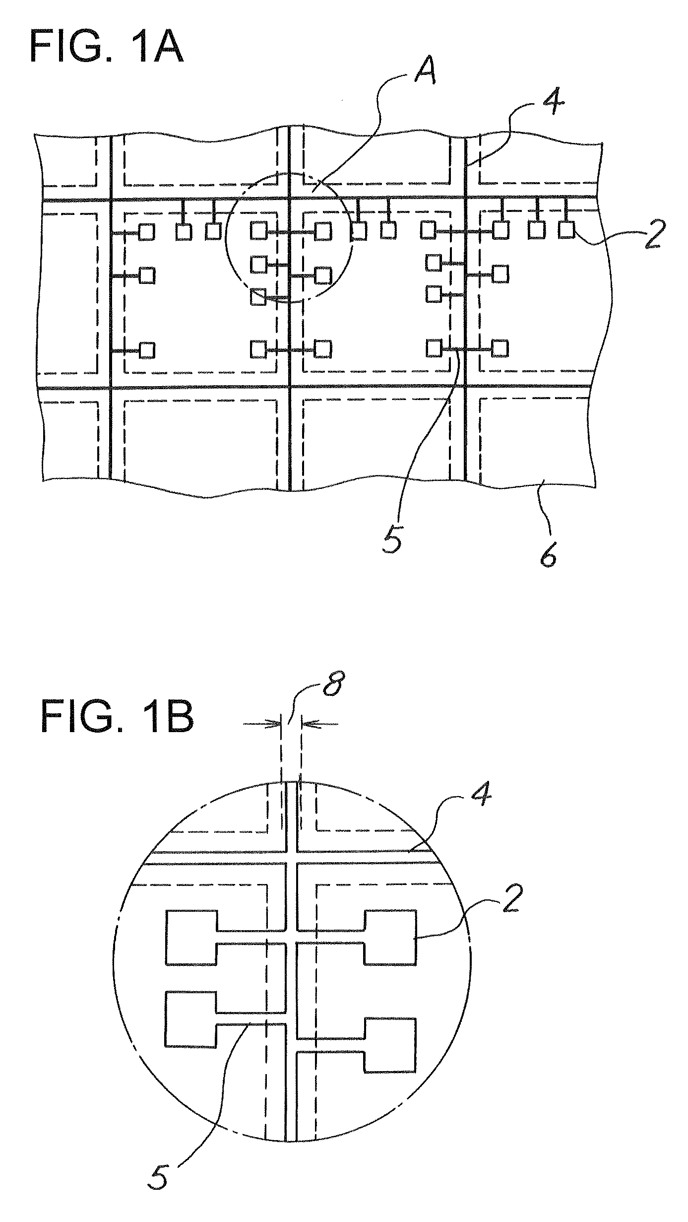
[0067]By means of this aspect, opposing first terminal electrodes can be connected over the shortest distance, so that feed lines are shortened, and the resistance values thereof are decreased.

Problems solved by technology

However, this method has the problem that, if the cutting position of the dicing saw (hereafter called the “dicer”) shifts slightly, insulation between bumps, that is, between terminals, cannot be secured.
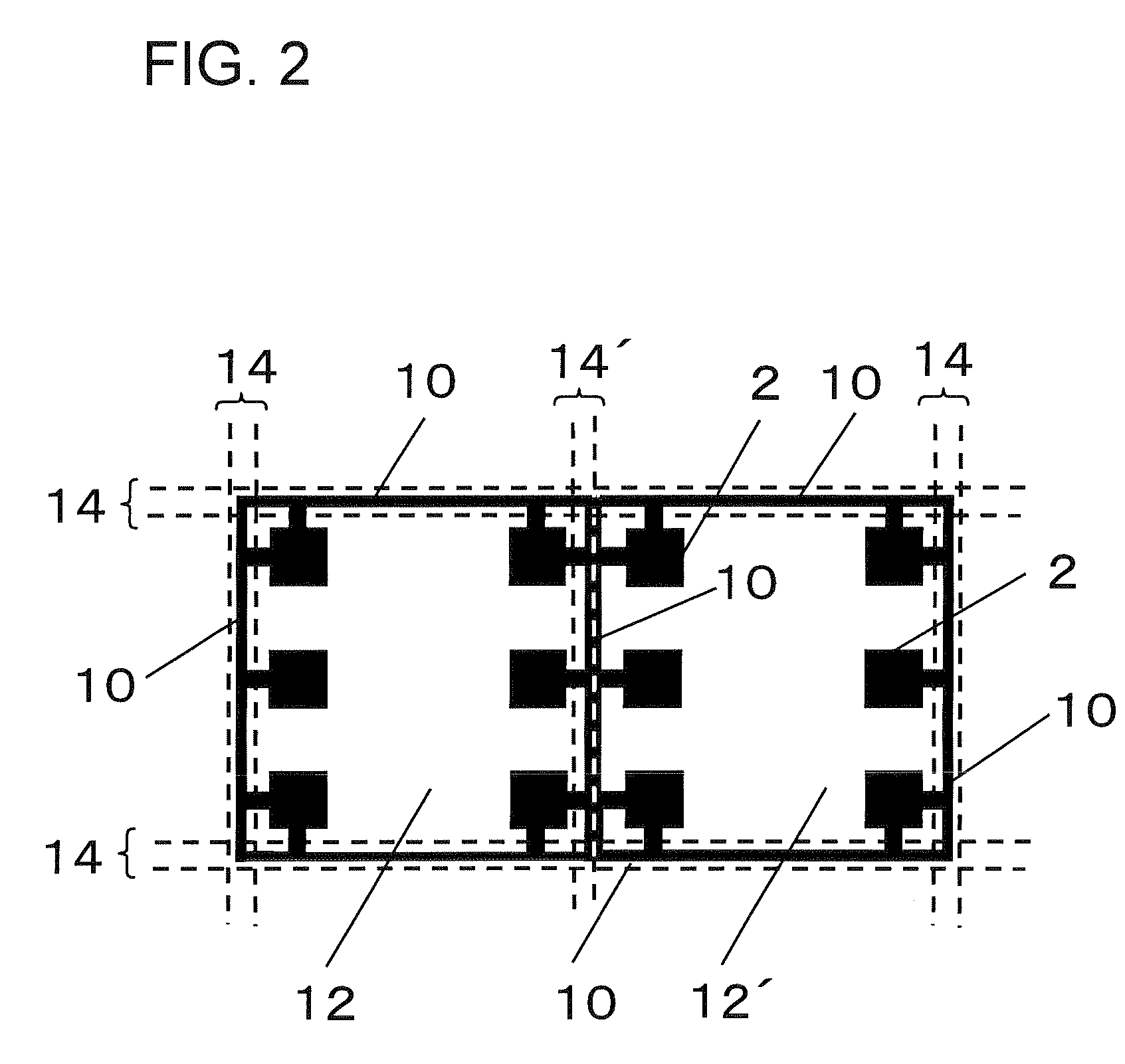
However, due to complexity of the drawing, these are omitted in FIG. 2.

Method used


Image

  • Electronic component and method of manufacturing the same
  • Electronic component and method of manufacturing the same
  • Electronic component and method of manufacturing the same

Examples


first embodiment

[0095]This embodiment relates to a surface acoustic wave device having feed lines which branch and one end of which reach the edge of the substrate, and a method of manufacture of such a component.

[0096]FIG. 4 is a plane view, seen through a resin layer covering the main surface of the piezoelectric substrate 24, of a surface acoustic wave device 22 of this embodiment. As shown in FIG. 4, in the surface acoustic wave device 22 of this embodiment, filters, reflectors, and other surface acoustic wave elements 26 are integrated. Also, the surface acoustic wave device 22 of this embodiment is packaged using WLCSP.

[0097]Below, the configuration of the surface acoustic wave device 22 of this embodiment is explained, with a description of the manufacturing procedure.

[0098](1) Manufacturing Procedure

[0099]FIG. 5 is a flow diagram showing the manufacturing procedure for the surface acoustic wave device 22 of this embodiment. FIG. 6 to FIG. 10 are process cross-sectional diagrams which explai...

second embodiment

[0176]This embodiment relates to a method of manufacture of an electronic component in which protrusions are provided on the side faces of dicing lines.

[0177]The method of manufacture of electronic components according to this embodiment is substantially the same as the method of manufacture of the first embodiment, except for the formation of a plurality of protrusions 82 on the side faces of dicing lines.

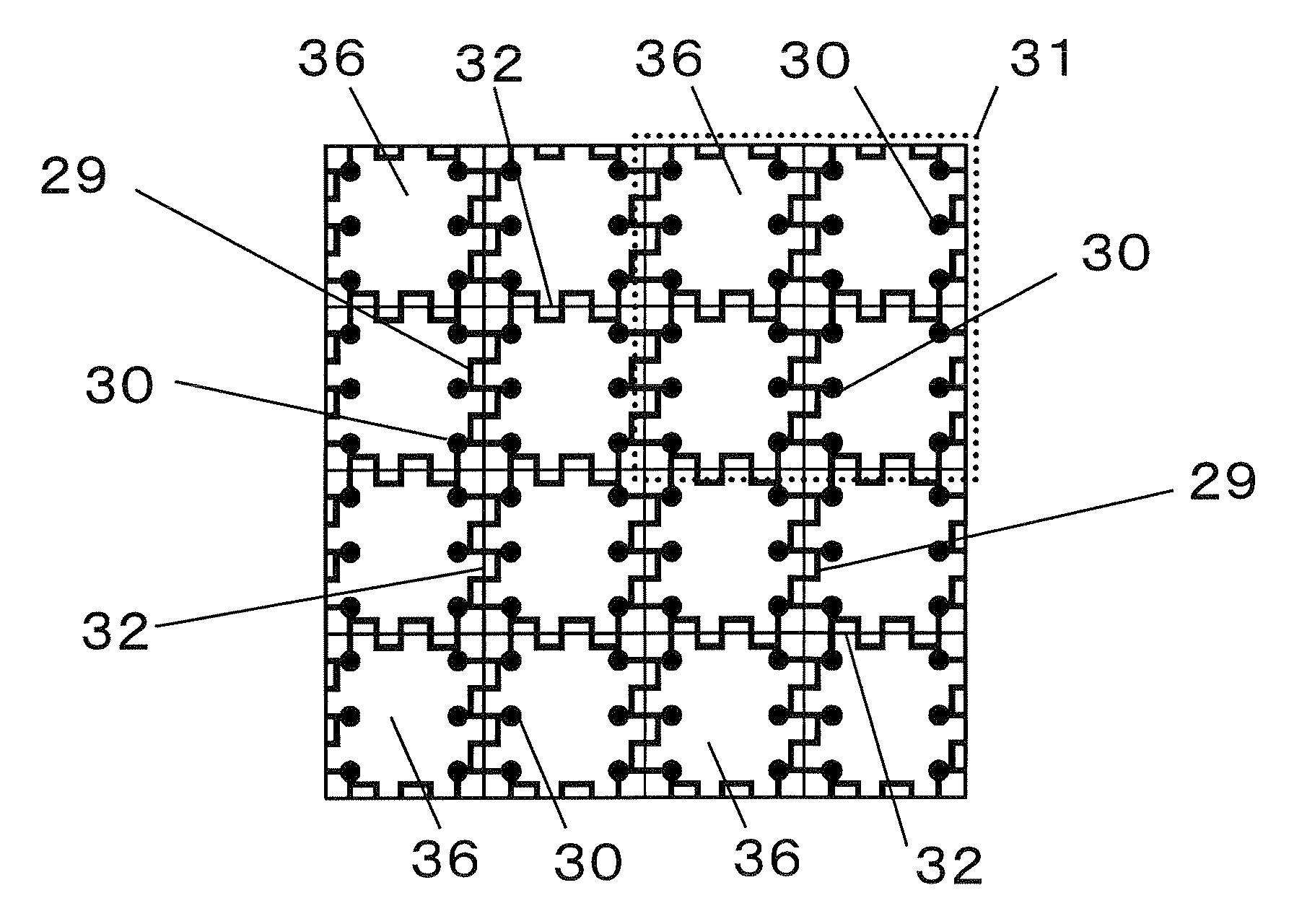
[0178]FIG. 17 is a plane view explaining dicing lines 32 formed on the outer periphery of the region 36 which is to become the electronic component. FIG. 18 is an enlarged view of the region A surrounded by the broken line in FIG. 17.

[0179]In this embodiment, as shown in FIG. 18, dicing lines having protrusions on side faces are formed. Hence when cutting the substrate to cut away electronic components, dicing lines can easily be distinguished from feed lines 29, and so productivity is improved.

[0180]The dicing lines 32 of this embodiment differ from the dicing lines of the first ...

modified example

[0191]FIG. 21 and FIG. 22 show a modified example of the first embodiment.

[0192]In the electronic component manufacturing method of the first embodiment, as shown in FIG. 14, feed lines 29 are formed having first portions 42 which connect in a straight line pairs of first terminal electrodes 40 arranged in direct opposition on either side of a first intended cutting region 34, and crank-shape second portions46 which branch from first portions 42.

[0193]However, the shape of feed lines formed in this invention is not limited to such shapes, and the second portions 46′ may be straight lines traversing the cutting region 14 diagonally, as in FIG. 22.

[0194]Further, in FIG. 14 the second portions 46 branch midway from the first portions 42, but may branch directly from the first terminal electrodes 30, as in FIG. 22.

[0195]Further, in the first and second embodiment, the substrate is a piezoelectric substrate, and surface acoustic wave elements are formed as functional elements. However, t...


PUM


Abstract

An electronic component includes a substrate, a functional element formed on the substrate, a plurality of terminals including a first terminal electrode connected to the functional element and a second terminal electrode layered on the first terminal electrode, and a feed line, one end of which is electrically connected to the first terminal electrode and the other end of which reaches an edge of the substrate, wherein the feed line includes a first portion directly reaching the edge, and a second portion branching from the first portion and then reaching the edge.

Description

CROSS-REFERENCE TO RELATED APPLICATIONS[0001]This application is based upon and claims the benefit of priority of the prior Japanese Patent Application No. 2008-44818, filed on Feb. 26, 2008, the entire contents of which are incorporated herein by reference.BACKGROUND OF THE INVENTION[0002]1. Field of the Invention[0003]This invention relates to an electronic component, terminals of which are formed thickly by electroplating, and to a method of manufacturing such electronic components.[0004]2. Description of the Related Art[0005]In recent years, there have been rapid advances in the miniaturization of portable telephones, transceivers, digital cameras, and other portable equipment. In response to such miniaturization of portable equipment, there have been strong demands for miniaturization of various electronic components which are the constituent components of such equipment (for example, surface acoustic wave (SAW) devices and other piezoelectric devices, integrated circuit (IC) d...

Claims


Application Information

Patent Timeline
IPC IPC(8): H01L23/538H01L21/70H01L21/301H01L21/3205H01L21/768H01L23/12H01L23/522H01L41/09H01L41/18H01L41/22H01L41/29H01L41/338H03H3/08H03H9/25
CPCH03H3/08H03H9/059H03H9/1092H01L2924/0002H01L2924/00
Inventor KANEDA, YASUFUMIMORIYA, AKIRASAKINADA, KAORUAIKAWA, SHUNICHIKONDOU, YOSHINORIYAMASHITA, TAKASHI
Owner TAIYO YUDEN KK
Learn More