
Carbon nanotube circuits design methodology

a carbon nanotube and circuit technology, applied in nanoinformatics, instruments, program control, etc., can solve the problems of not being able to adjust the width of carbon nanotubes similarly to that of a typical mosfet, the direct synthesis and growth of one-dimensional nanostructures has been relatively slow, and the effect of known carbon nanotube fabrication processes

Inactive Publication Date: 2009-08-27
MOTOROLA INC
View PDF4 Cites 27 Cited by
  • Summary
  • Abstract
  • Description
  • Claims
  • Application Information

AI Technical Summary

Problems solved by technology

In contrast with zero-dimensional, e.g., quantum dots, and two-dimensional nanostructures, e.g., GaAs / AlGaAs superlattice, direct synthesis and growth of one-dimensional nanostructures has been relatively slow due to difficulties associated with controlling the chemical composition, dimensions, and morphology.
However the catalytic nanoparticles usually are derived by a wet slurry route which typically has been difficult to use for patterning small features.
Known carbon nanotube fabrication processes suffer due to a lack of flexible design parameters.
However, the width of the carbon nanotube may not be adjusted similarly to that of a typical MOSFET because the diameter of the carbon nanotube is often fixed for a particular carbon nanotube growth process.
In addition, the diameter of the nanotube determines its bandgap, which affects the threshold voltage and contact resistance, thereby affecting the operation of the carbon nanotube FET.
Multiple parallel carbon nanotube FETs, while possibly providing the necessary current output, requires an inefficient use of area on the integrated circuit.

Method used


Image

  • Carbon nanotube circuits design methodology
  • Carbon nanotube circuits design methodology
  • Carbon nanotube circuits design methodology

Examples


Embodiment Construction

[0019]The following detailed description of the invention is merely exemplary in nature and is not intended to limit the invention or the application and uses of the invention. Furthermore, there is no intention to be bound by any theory presented in the preceding background of the invention or the following detailed description of the invention.

[0020]One-dimensional nanostructures such as nanotubes and nanowires show promise for the development of molecular-scale transistors used in, e.g., resonators and logic / memory elements. One-dimensional nanostructures are herein defined as a material having a high aspect ratio of greater than 10 to 1 (length to diameter) and includes, either single or bundled, at least carbon nanotubes with a single wall or a limited number of walls, carbon nanofibers, carbon nanowires, and semiconducting nanowires.

[0021]A mapping process is described herein including three exemplary embodiments. The first exemplary embodiment comprises adjusting a width of t...


PUM


Abstract

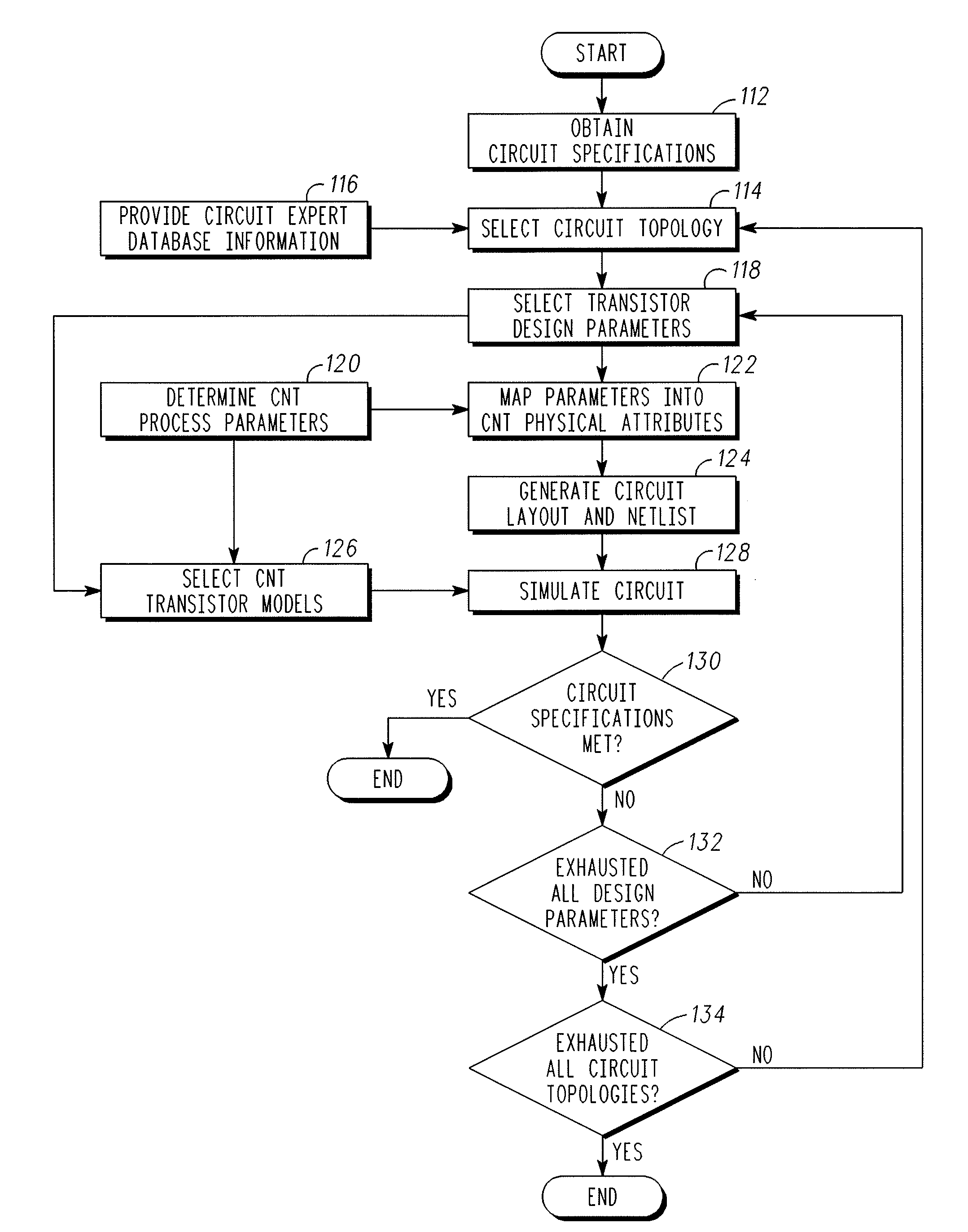
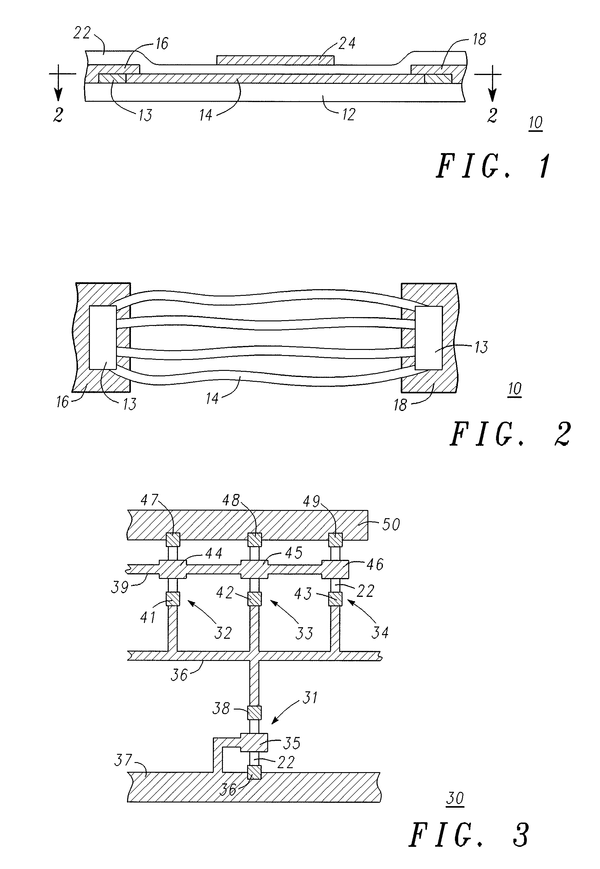
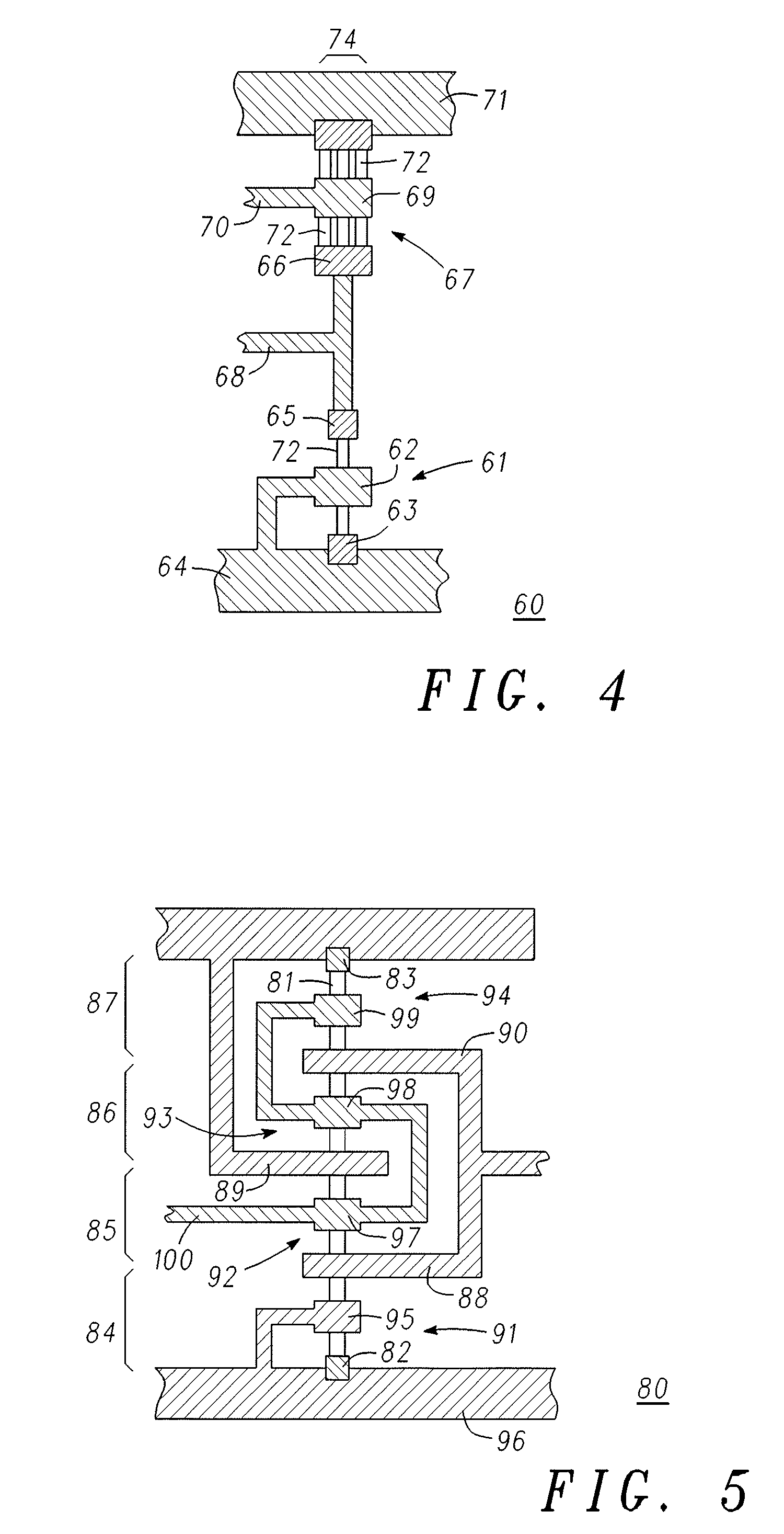
A methodology is provided for optimizing circuit parameters of circuits including carbon nanotube transistors. The method comprises mapping (122) selected transistor design parameters (118), based on carbon nanotube process parameters (120) and selected circuit topologies (114), into carbon nanotube physical attributes. A circuit layout is generated (124) from the carbon nanotube physical attributes and simulated (128). The steps are repeated until circuit specifications (130) are met. The carbon nanotube physical attributes may include, for example, the catalyst width (74) for growing a plurality of carbon nanotubes (72) or number of segments in a serpentine electrode structure (88, 89, 90) contacting a single carbon nanotube (81).

Description

FIELD OF THE INVENTION[0001]The present invention generally relates to electronic circuitry and more particularly to a methodology for optimizing circuit parameters of circuits including carbon nanotube transistors.BACKGROUND OF THE INVENTION[0002]One-dimensional nanostructures, such as belts, rods, tubes and wires, have become the focus of intensive research with their own unique applications. One-dimensional nanostructures are model systems to investigate the dependence of electrical and thermal transport or mechanical properties as a function of size reduction. In contrast with zero-dimensional, e.g., quantum dots, and two-dimensional nanostructures, e.g., GaAs / AlGaAs superlattice, direct synthesis and growth of one-dimensional nanostructures has been relatively slow due to difficulties associated with controlling the chemical composition, dimensions, and morphology. Alternatively, various one-dimensional nanostructures have been fabricated using a number of advanced nanolithogra...

Claims


Application Information

Patent Timeline
IPC IPC(8): G06F17/50
CPCB82Y10/00G06F17/5045H01L23/53276H01L51/0048H01L2924/0002H01L2924/00G06F30/30H10K85/221
Inventor LEE, KING F.AMLANI, ISLAMSHAH S.
Owner MOTOROLA INC
Learn More