Substrate heating apparatus, semiconductor device manufacturing method, and semiconductor device

Inactive Publication Date: 2009-09-03
CANON ANELVA CORP
View PDF6 Cites 14 Cited by
  • Summary
  • Abstract
  • Description
  • Claims
  • Application Information

AI Technical Summary

Benefits of technology

[0013]It is an object of the present invention to provide a substrate heating apparatus in which the internal pressure of a conductive heater can be maintained at the regulated val

Problems solved by technology

This may sharply, undesirably increase the internal pressure of the conductive heater.
This sharp temper

Method used


Image

  • Substrate heating apparatus, semiconductor device manufacturing method, and semiconductor device
  • Substrate heating apparatus, semiconductor device manufacturing method, and semiconductor device
  • Substrate heating apparatus, semiconductor device manufacturing method, and semiconductor device

Examples


Embodiment Construction

[0029]The best embodiment to practice the present invention will be described hereinafter with reference to the accompanying drawings.

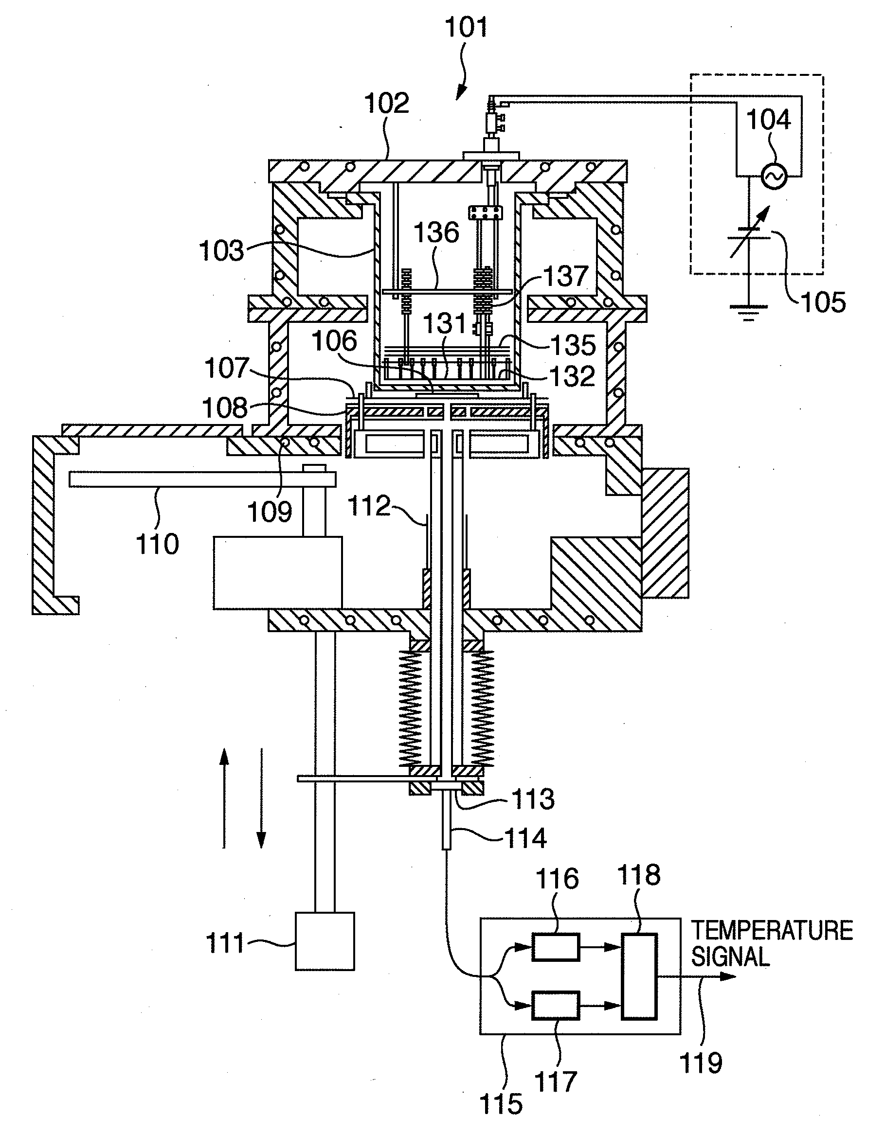
[0030]FIG. 1 is a sectional view showing a substrate heating apparatus according to an embodiment of the present invention.

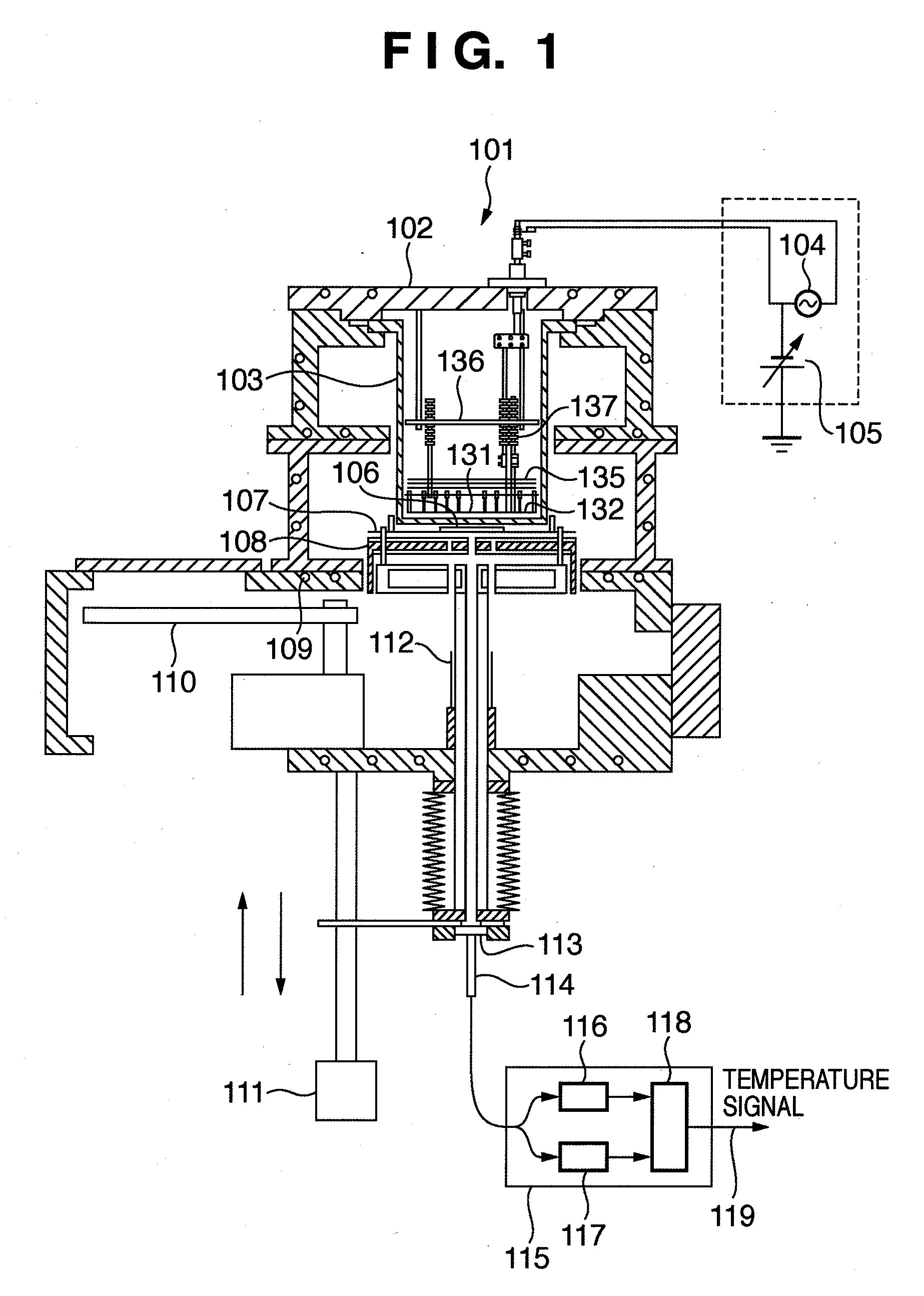
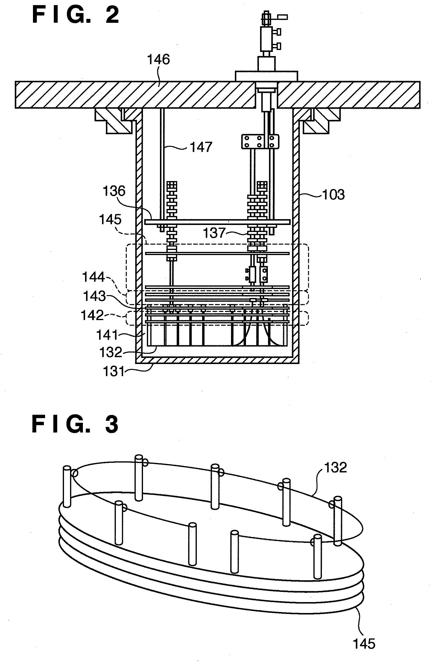
[0031]As shown in FIG. 1, a substrate heating apparatus 101 of this embodiment includes a vacuum chamber 102, vacuum heating vessel 103, filament power supply 104, high-voltage power supply 105, substrate 106, substrate stage 107, and substrate holding table 108. The substrate heating apparatus 101 also includes a carbon conductive heater 131, water-cooling channel 109, water-cooled shutter 110, moving mechanism 111, and lift pins 112. The substrate heating apparatus 101 further includes a two-wavelength-type radiation thermometer 115, wavelength detection element a 116, wavelength detection element b 117, arithmetic circuit 118, temperature signal 119, condensing portion 114, and transmission window 113. The substrate heating app...


PUM


Abstract

In a substrate heating apparatus, thermoelectrons generated by a filament (132) in a vacuum heating vessel (103) are accelerated to collide against a conductive heater (131) which forms one surface of the vacuum heating vessel (103), thus generating heat. The conductive heater (131) is made of carbon. At least one of the inner and outer surfaces of the conductive heater (131) is coated with tantalum carbide (TaC).

Description

BACKGROUND OF THE INVENTION[0001]1. Field of the Invention[0002]The present invention relates to a substrate heating apparatus, semiconductor device manufacturing method, and semiconductor device.[0003]2. Description of the Related Art[0004]In general, a semiconductor device manufacturing technique frequently requires a process for heating a semiconductor substrate quickly.[0005]In particular, activation annealing of a wide bandgap semiconductor represented by silicon carbide (SiC) as disclosed in non-patent reference 1 (T. Kimoto, N. Inoue and H. Matsunami: Phys. Stat. Sol. (a) Vol. 162 (1997), p. 263) generally requires a high temperature of 1,600° C. or more.[0006]In such annealing, when forming an aluminum-implanted p-well, it is very important in terms of the reliability of a semiconductor device to electrically activate the implanted impurity by 100%, thus restoring complete crystals.[0007]To raise such an activation annealing process to the industrial level, it is necessary t...

Claims


Application Information

Patent Timeline
IPC IPC(8): H01L29/24H01L21/67H01L21/04
CPCH01L21/046H01L21/67115H01L21/67103H01L21/67098
Inventor SHIBAGAKI, MASAMI
Owner CANON ANELVA CORP
Why Eureka
Try Eureka