Planar antenna and manufacturing method thereof
a technology of planar antenna and manufacturing method, which is applied in the direction of resonant antenna, waveguide type devices, instruments, etc., can solve the problems of difficult to lower costs, easy instability of communication properties of antennas, and deterioration of adhesiveness of metal-plated layers, so as to reduce the communication property in long-term use, good communication properties, and stable communication properties
- Summary
- Abstract
- Description
- Claims
- Application Information
AI Technical Summary
Benefits of technology
Problems solved by technology
Method used
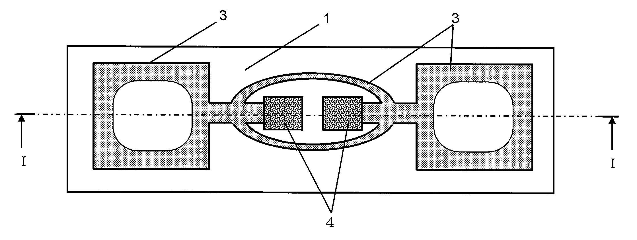
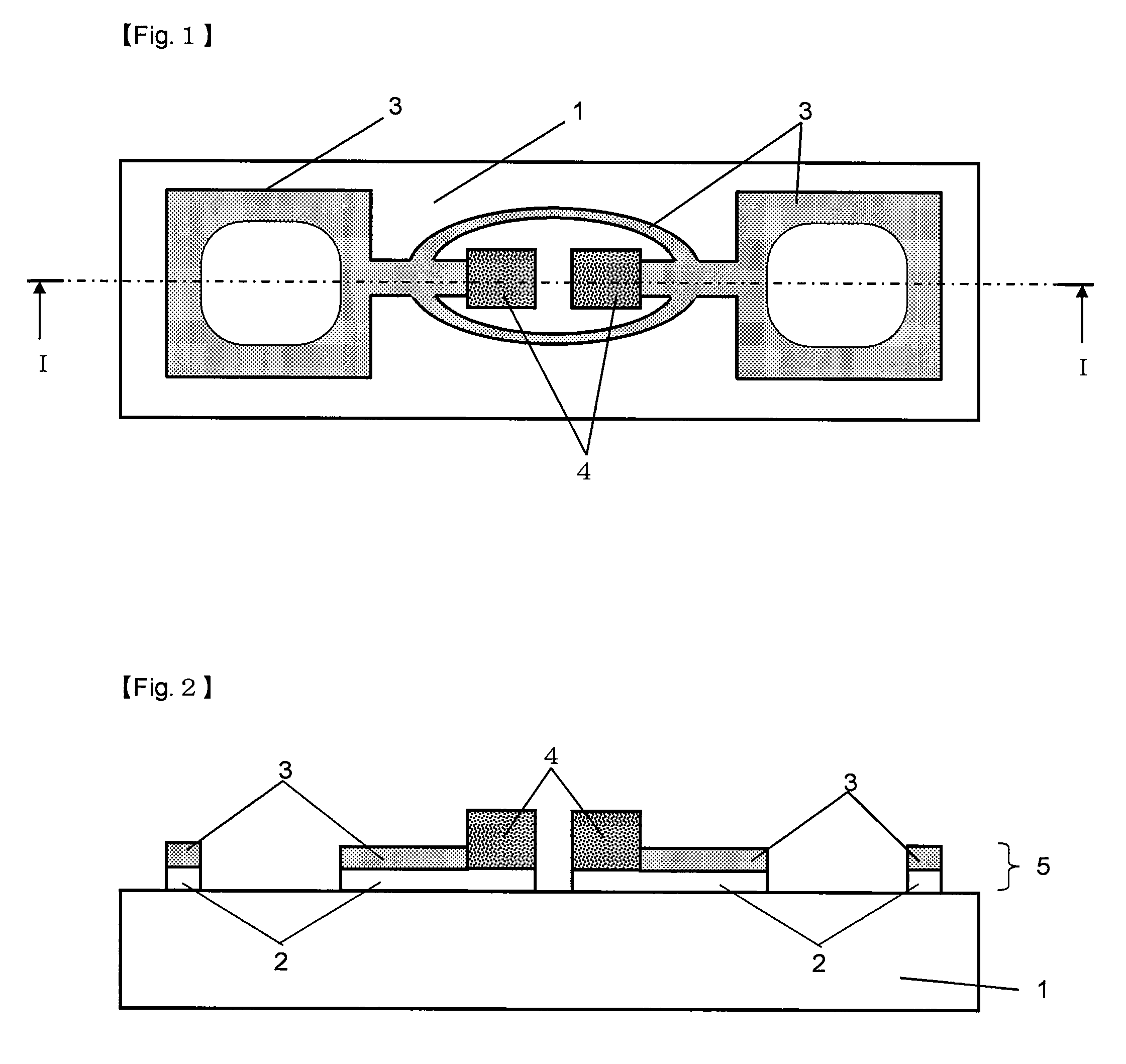
Image

Examples
example 1
[0094]Using a 75 μm thick biaxially oriented polyethylene terephthalate film (Lumirror S56 manufactured by Toray Industries, Inc.) as a plastic film, a 3 μm thick metal layer containing 99.99% aluminum was formed on one side of the biaxially oriented film with an induction heating type vacuum deposition device. At this time, the vacuum deposition was performed under a vacuum of 1 to 5×10⁻⁶ Torr by controlling the voltage and current of an induction heating furnace, setting a traveling speed of the film in vacuum deposition to 1 m / min so that the thickness of the aluminum vacuum deposition layer becomes 3 μm.
[0095]In order to form a protective layer on the aluminum metal layer obtained in this way, a circuit pattern was screen-printed with a printing plate T-250 mesh using a printing ink (TETRON 990 Black manufactured by Jujo Chemical Co., Ltd.), and then heated and dried at 90° C. for 1 minute. Next, in order to form a heat-sealable conductive layer, a connection terminal part was p...
example 2
[0100]The planar antenna was produced with the same method as Example 1 except that only the protective layer at the surface layer of antenna part of the planar antenna produced in Example 1 was removed with a paint remover in the above-described evaluation method 1. The surface resistance value of the metallic vacuum deposition layer, the surface resistance value of the conductive layer, the breaking bend durability, and the durability of the hot & high humidity environment of the obtained planar antenna are shown in Table 1. Both the breaking bend durability and the durability of the hot & high humidity environment were good.
[0101]Further, similarly to Example 1, a PET film (Toray Industries, Inc. “Lumirror (registered trademark)” S10) was pasted at a temperature of 100° C., and then bending was repeated with a method used in the above-described breaking bend durability. The PET film pasted to the antenna part had been peeled a little although it was at a level not causing a pract...
PUM
| Property | Measurement | Unit |
|---|---|---|
| thickness | aaaaa | aaaaa |
| thickness | aaaaa | aaaaa |
| RH | aaaaa | aaaaa |
Abstract
Description
Claims
Application Information
 - R&D
- Intellectual Property
- Life Sciences
- Materials
- Tech Scout
- Unparalleled Data Quality
- Higher Quality Content
- 60% Fewer Hallucinations
Browse by: Latest US Patents, China's latest patents, Technical Efficacy Thesaurus, Application Domain, Technology Topic, Popular Technical Reports.
© 2025 PatSnap. All rights reserved.Legal|Privacy policy|Modern Slavery Act Transparency Statement|Sitemap|About US| Contact US: help@patsnap.com