Unlock instant, AI-driven research and patent intelligence for your innovation.
Non-volatile memory and-array
Inactive Publication Date: 2009-09-10
NXP BV
View PDF9 Cites 1 Cited by
Summary
Abstract
Description
Claims
Application Information
AI Technical Summary
This helps you quickly interpret patents by identifying the three key elements:
Problems solved by technology
Method used
Benefits of technology
Benefits of technology
[0015]It is an object of the present invention to reduce the effect of gate disturb in SONOS based AND-array memory.
[0017]Advantageously, the differential configuration of the non-volatile memory cell allows to determine the bit value of a memory cell from the relative difference of the threshold voltage VT of two memory transistors which during the lifetime of the memory experience the same disturbs. Since the two transistors are subjected to the same disturbs, the effect on their threshold voltage VT will be similar. By measuring the threshold voltage VT of each of the two transistors and by taking the difference between the measured threshold voltages the bit value of the memory cell may be determined. The differential measurement thus allows to ignore a change of threshold voltage due to disturb.
[0020]Advantageously, the arrangement allows to create a non-volatile memory cell which relatively reduces the occupied area size by about 25%.
Problems solved by technology
The charge trapping properties of the siliconnitride layer allow for downscaling the thickness of the tunnel-oxide layer, which may result in lower program / erase voltages.
Disadvantageously, SONOS memory devices suffer from a gate disturb effect, for example during the read action.
Gate disturb relates to a disturbance of a threshold voltage VT of a memory cell and is caused by exposure to a relatively large voltage difference between the channel region of the cell and the control gate, leading to a relatively large electric field in the ONO stack, which can gradually change the charge in the nitride by soft programming or soft erase.
For example, gate disturb due to the application of a voltage on the control gate of the memory cell during a read operation may cause a slow programming of the memory cell, i.e., some tunneling takes place during reading.
Also, in comparison to non-volatile memory devices based on a floating gate, SONOS memory devices suffer from a relatively low data retention capability.
Method used
Image
Click on the blue label to locate the original text in one second.
Reading with bidirectional positioning of images and text.
Examples
first embodiment
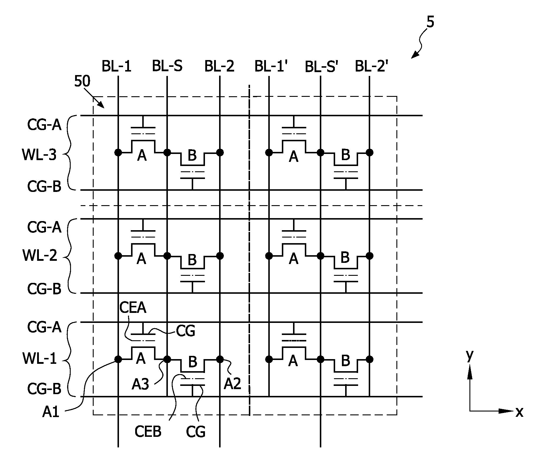
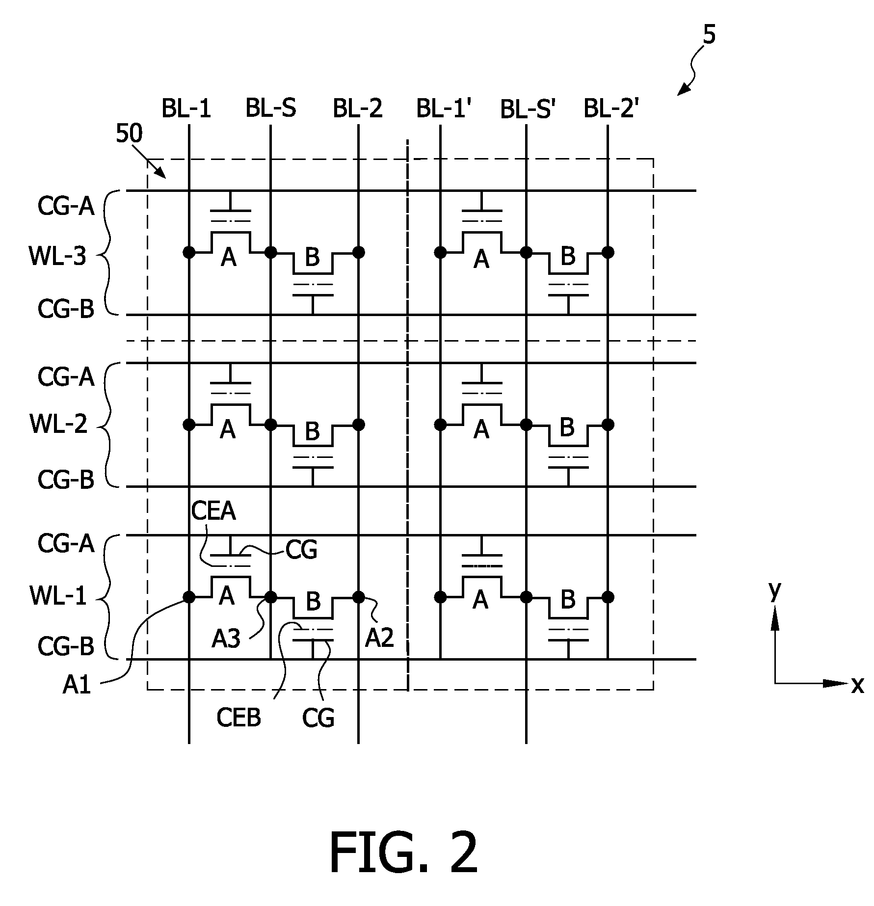
[0076]FIGS. 3a, 3b, 3c show a top view of an arrangement of non-volatile memory cells in the AND-array according to a
[0077]The non-volatile memory cells 50, 50′, 50″, 50′″ are arranged on a semiconductor substrate 100.
[0078]In FIG. 3a the arrangement of two adjacent non-volatile memory cells 50, 50′ is shown on a level of a zero layer (i.e., the surface of the semiconductor substrate). The non-volatile memory cells 50, 50′ are schematically demarcated by dashed-line rectangles.
[0079]In the arrangement two non-volatile memory cells 50, 50′ adjacent in the first direction X are shown, and two non-volatile memory cells 50″, 50′″ adjacent in the second direction Y (at a non-zero angle with the first direction X).
[0080]Each non-volatile memory cell 50; 50′ comprises a first diffusion region A1; A1′ and a second diffusion region A2; A2′ which are to be connected to the first bit line BL-1; BL-1′ and the second bit line BL-2; BL-2′, respectively.
[0081]In between the first diffusion region ...
second embodiment
[0129]FIGS. 8a, 8b, 8c, 8d show a top view of an arrangement of memory cells in the AND-array at different stages of the production process.
[0130]In FIG. 8a the arrangement of non-volatile memory cells is shown on a level of the zero layer (i.e., the surface of the semiconductor substrate). By way of example, three areas 75, 75′, 75″ are shown that each comprise a non-volatile memory cell. The areas 75, 75′, 75″ are adjacent to each other in the direction X. Each non-volatile memory cell 75; 75′; 75″ is demarcated by a dashed-line rectangle.
[0131]Each non-volatile memory cell 75; 75′; 75″ comprises a first diffusion region A1; A1′; A1″ and a second diffusion region A2; A2′; A2″ which are to be connected to the first bit line BL-1; BL-1′; BL-1″ and the second bit line BL-2; BL-2′; BL-2″, respectively.
[0132]In between the first diffusion region A1; A1′; A1″ and the second diffusion region A2; A2′; A2″ a common diffusion region A3; A3′; A3″ is arranged which is connected to the sensin...
PUM
Abstract
A non-volatile memorycell on a semiconductor substrate includes a first and a second transistor. Each transistor is arranged as a memory element that includes two diffusion regions capable of acting as either source or drain, a charge storage element and a control gate element. A channel region is located intermediate the two diffusion regions. The charge storage element is located over the channel region, the control gate element is arranged on top of the charge storage element. One diffusion region of the first transistor and one diffusion region of the second transistor form a common diffusion region. The other diffusion region of the first transistor is connected as first diffusion region to a first bit line, the other diffusion region of the second transistor is connected as second diffusion region to a second bit line and the common diffusion region is connected to a sensing line.
Description
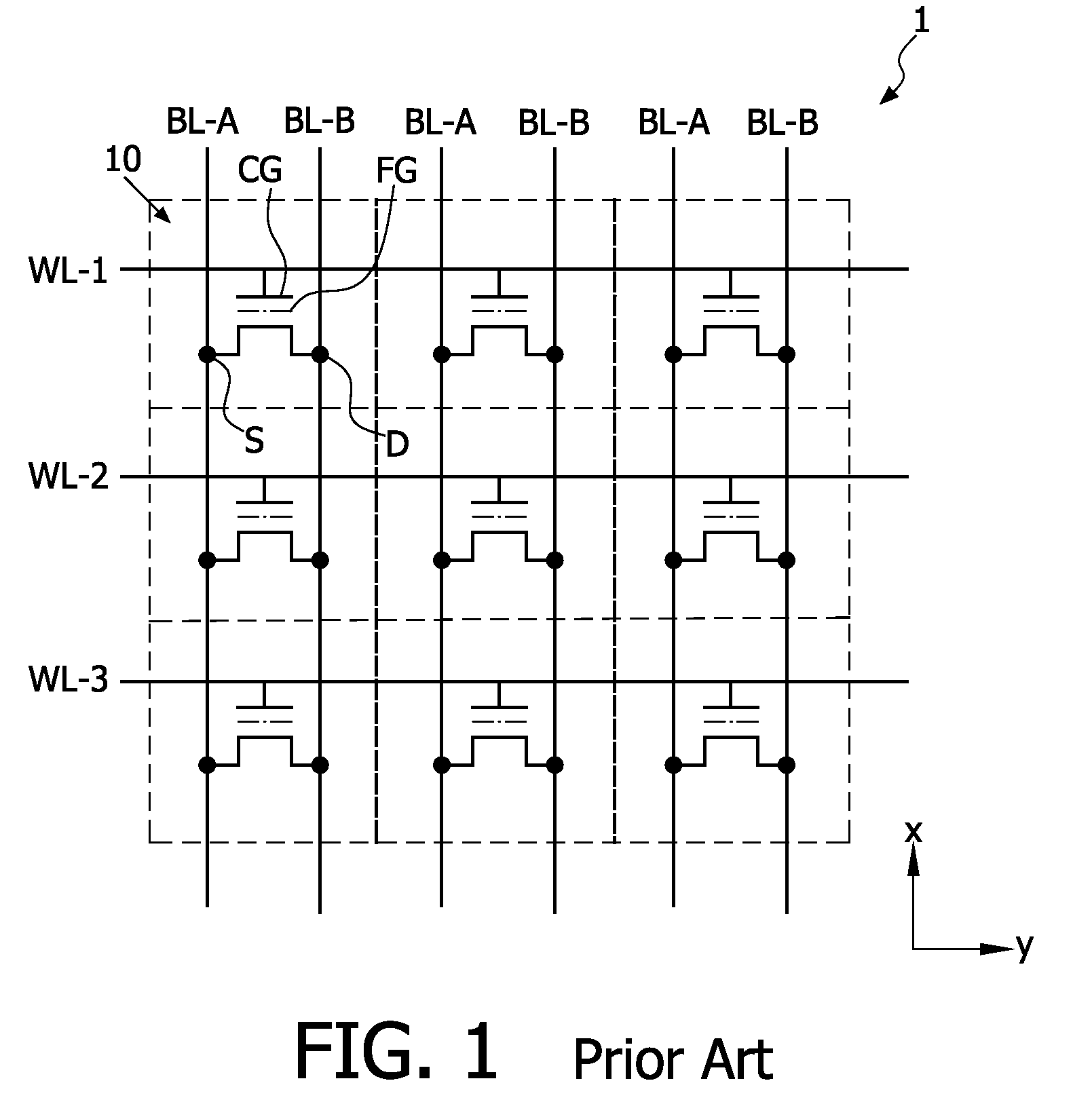
FIELD OF THE INVENTION[0001]The present invention relates to a non-volatile memorycell. Also, the present invention relates to a non-volatile memory AND-array. Moreover, the present invention relates to a layout of such a non-volatile memory AND-array. Further, the present invention relates to a method of operating such a non-volatile memory AND-array.BACKGROUND OF THE INVENTION[0002]A non-volatile memory AND-array is known from international application WO 94 / 10686.[0003]The AND-array comprises a plurality of memory cells which each consist of a stacked gate transistor comprising a floating gate which is capable of storing electric charge and a control gate which is capable to control operations on the floating gate, i.e., reading, writing, and erasing.[0004]In the AND-array configuration, the memory cells are arranged in rows and columns. Memory cells in the same row share a word-line which is connected to each of their control gates. Memory cells in the same column share one bit...
Claims
Application Information
Patent Timeline
Application Date:The date an application was filed.
Publication Date:The date a patent or application was officially published.
First Publication Date:The earliest publication date of a patent with the same application number.
Issue Date:Publication date of the patent grant document.
PCT Entry Date:The Entry date of PCT National Phase.
Estimated Expiry Date:The statutory expiry date of a patent right according to the Patent Law, and it is the longest term of protection that the patent right can achieve without the termination of the patent right due to other reasons(Term extension factor has been taken into account ).
Invalid Date:Actual expiry date is based on effective date or publication date of legal transaction data of invalid patent.
