Solid-state imaging device

a solid-state imaging and imaging layer technology, applied in the direction of radiation control devices, semiconductor devices, electrical apparatus, etc., can solve the problem of impurity diffusion in previously formed impurity layers

Active Publication Date: 2009-09-17
SONY CORP
View PDF2 Cites 21 Cited by
  • Summary
  • Abstract
  • Description
  • Claims
  • Application Information

AI Technical Summary

Benefits of technology

[0015]There is a need for the present invention to provide a solid-state imaging device which does not need the hole accumulation layer (which is an impurity diffusion layer requiring high-temperature heat treatment) to reduce dark current arising from the interface state and which has the sensor formed at a shallow position in the semiconductor substrate for efficient charge transfer.
[0017]In the solid-state imaging device constructed as mentioned above, the interfacial layer produces dipoles, with one side (adjacent to the negative charge accumulation layer) positively charged and the other side (adjacent to the sensor or the semiconductor substrate) negatively charged. The resulting dipoles produce negative bias in the negative charge accumulation layer, thereby effectively attracting positive charges to the surface of the semiconductor substrate to form the hole accumulation layer that compensates the interface state.
[0018]The solid-state imaging device according to the embodiment of the present invention has an interfacial layer between the sensor formed on the semiconductor substrate and the negative charge accumulation layer. This interfacial layer generates dipoles therein that effectively attract positive charges to the surface of the semiconductor substrate, thereby forming the hole accumulation layer that compensates the interface state. Therefore, it constitutes the HAD structure to prevent dark current without the necessity of forming on the sensor surface the hole accumulation layer which is an impurity diffusion layer that needs high-temperature heat treatment. The result is that the sensor can be formed shallow in the surface of the semiconductor substrate and charges can be transferred efficiently to the floating diffusion arranged through the gate electrode adjacent to the sensor.

Problems solved by technology

In other words, it involves difficulties in forming the hole accumulation layer 104 by a low-temperature process below 400° C. Moreover, high-temperature annealing above 700° C. inevitably causes diffusion of impurities in previously formed impurity layers.

Method used


Image

  • Solid-state imaging device
  • Solid-state imaging device
  • Solid-state imaging device

Examples


Embodiment Construction

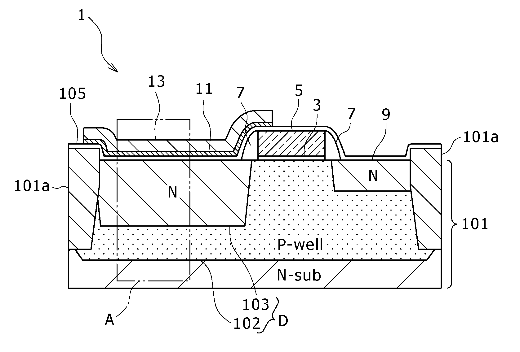
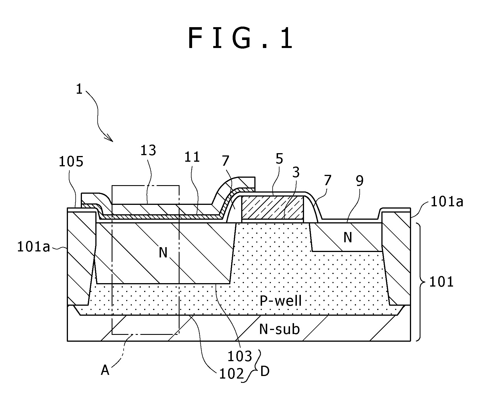
[0023]The following is a detailed description of the solid-state imaging device according to an embodiment of the present invention shown in the accompanying drawings, in which the same constituents as in FIG. 4 are given the same symbols.

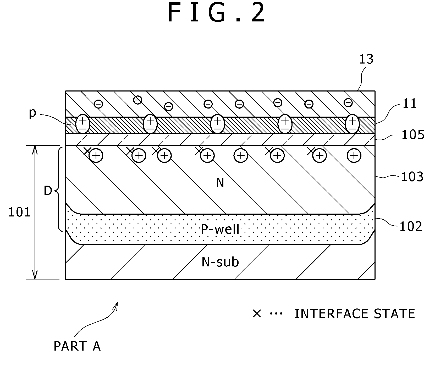
[0024]FIG. 1 is a sectional view showing important parts of a solid-state imaging device 1 according to the embodiment of the present invention. The solid-state imaging device 1 contains a CMOS sensor, and the figure represents the sensor for one pixel. FIG. 2 is an enlarged view showing part A in FIG. 1. As shown in these figures, the solid-state imaging device 1 is one which contains a sensor of HAD structure and is constructed as follows.

[0025]The semiconductor substrate 101 is formed from N-type single-crystal silicon. It is divided into individual pixel regions by the shallow trench isolation (STI) 101a. That part of the semiconductor substrate 101 which corresponds to each pixel region divided by the isolation 101a has the P-well diffusion la...


PUM


Abstract

Disclosed herein is a solid-state imaging device including: a semiconductor substrate; a sensor of impurity diffusion layer formed on the surface layer of said semiconductor substrate; a negative charge accumulation layer formed on said sensor from an insulating material containing a first metallic substance; and an interfacial layer formed between said sensor and said negative charge accumulation layer from an insulating material containing a second metallic substance having greater electronegativity than said first metallic substance.

Description

CROSS REFERENCES TO RELATED APPLICATIONS[0001]The present invention contains subject matter related to Japanese Patent Application JP 2008-062487 filed in the Japan Patent Office on Mar. 12, 2008, the entire contents of which being incorporated herein by reference.BACKGROUND OF THE INVENTION[0002]1. Field of the Invention[0003]The present invention relates to a solid-state imaging device and, more particularly, to a solid-state imaging device capable of compensating the interface state of the surface of a semiconductor substrate with photoelectric converting sensors formed thereon.[0004]2. Description of the Related Art[0005]Video cameras and digital still cameras are commonly equipped with a solid-state imaging device composed of CCD (Charge Coupled Device) or CMOS (Complementary Metal Oxide Semiconductor) image sensors. Solid-state imaging devices of any kind have important problems with sensitivity improvement and noise reduction.[0006]Noise involved in solid-state imaging device...

Claims


Application Information

Patent Timeline
Patent Type & Authority Applications(United States)
IPC IPC(8): H01L31/00H01L31/0216
CPCH01L31/103H01L27/14609
Inventor TAKIMOTO, KAORI
Owner SONY CORP
Why Eureka
Try Eureka