

Light-Emitting Element, Light-Emitting Device, and Electronic Appliance
- Summary
- Abstract
- Description
- Claims
- Application Information
AI Technical Summary
Benefits of technology
Problems solved by technology
Method used
Image

Examples
embodiment mode 1
[0102]This embodiment mode will describe a composite material which is used for a light-emitting element of the present invention. In this specification, being composite means not only a simple mixture of two materials but also a change into such a state that charges are transported between two materials through a mixture of the materials at a molecular level.
[0103]The composite material used in the present invention is a composite material of a first organic compound and an inorganic compound. As the first organic compound for the composite material, various compounds such as an aromatic amine compound, a carbazole derivative, aromatic hydrocarbon, and a high-molecular compound (such as oligomer, dendrimer, or polymer) can be used. The first organic compound used for the composite material is preferably an organic compound having a high hole-transporting property. Specifically, a substance having a hole mobility of 10−6 cm2 / Vs or higher is preferably used. However, other substances...
embodiment mode 2
[0116]This embodiment mode will describe a layer containing a second organic compound, which is provided so as to be in contact with the composite material of the first organic compound and the inorganic compound shown in Embodiment Mode 1.
[0117]The second organic compound in the layer containing the second organic compound, which is provided so as to be in contact with the layer containing the composite material, does not have an absorption peak in a wavelength region of 450 to 800 nm, in the case where the second organic compound is compounded with the inorganic compound in the composite material. A composite material containing the second organic compound and the inorganic compound with the same mixture ratio as the first organic compound and the inorganic compound of the layer containing the composite material has a transmittance of 80% or higher in a wavelength region of 450 to 800 nm when the film thickness is 100 nm.
[0118]As the second organic compound, various compounds such...
embodiment mode 3
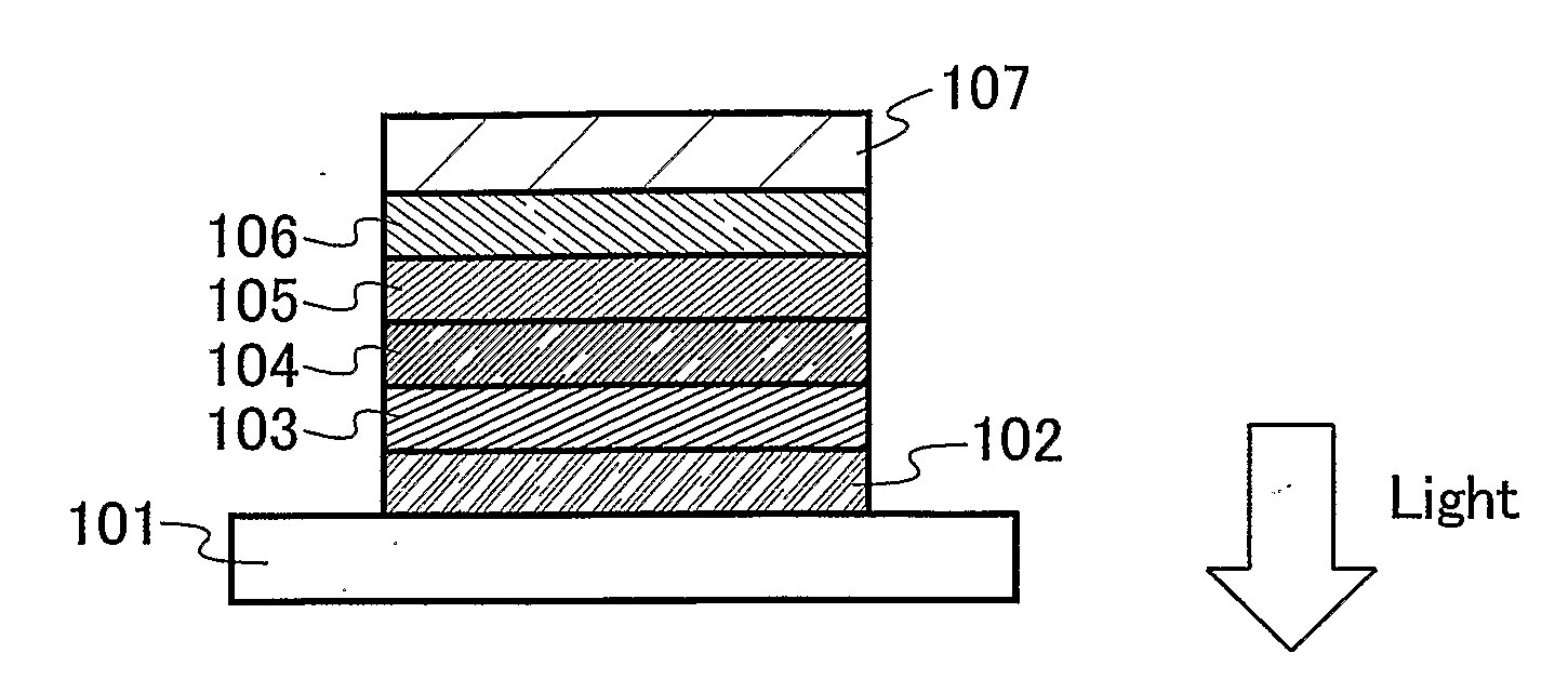
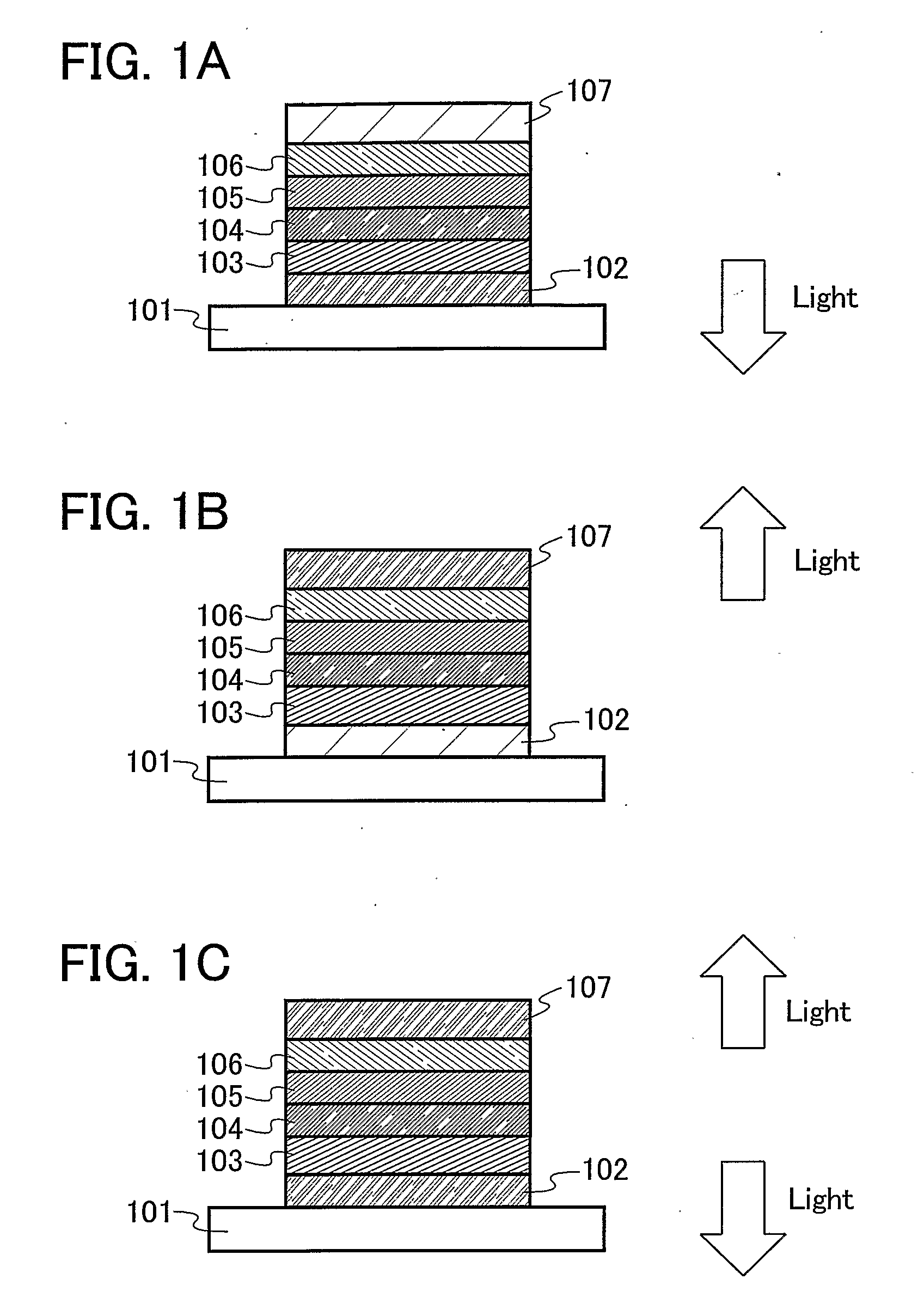
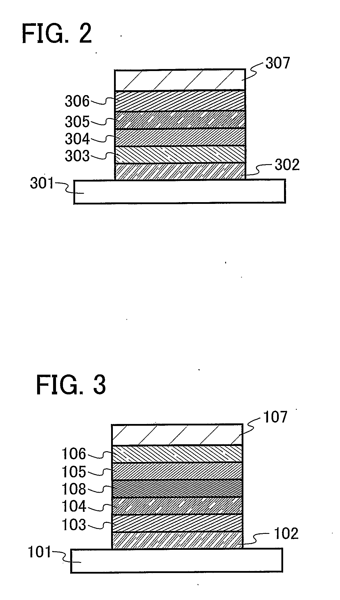
[0126]A light-emitting element of the present invention has a plurality of layers between a pair of electrodes. The plurality of layers are stacked by combining layers which contain a substance having a high carrier-injecting property and a substance having a high carrier-transporting property so that a light-emitting region is formed apart from the electrodes, i.e., so that carries are recombined at a portion away from the electrodes.
[0127]A mode of a light-emitting element of the present invention will be hereinafter described with reference to FIG. 1A.
[0128]In this embodiment mode, the light-emitting element includes a first electrode 102; a first layer 103, a second layer 104, a third layer 105, and a fourth layer 106 which are stacked sequentially over the first electrode 102; and a second electrode 107 provided over the fourth layer 106. In this embodiment mode, the first electrode 102 functions as an anode and the second electrode 107 functions as a cathode.
[0129]The substrat...
PUM
 Abstract
Description
Claims
Application Information