Thin film transistor and display device

a thin film transistor and display device technology, applied in the direction of semiconductor devices, basic electric elements, electrical appliances, etc., can solve the problems of high manufacturing cost, insufficient switching characteristics, low field-effect mobility and small on-state current, etc., to achieve large on-state current, increase field-effect mobility, and reduce off-state current

Inactive Publication Date: 2009-09-24
SEMICON ENERGY LAB CO LTD
View PDF46 Cites 26 Cited by
  • Summary
  • Abstract
  • Description
  • Claims
  • Application Information

AI Technical Summary

Benefits of technology

[0011]A thin film transistor in which a polycrystalline silicon layer is used for a channel formation region has characteristics such as much higher field-effect mobility and larger on-state current than the aforementioned two types of thin film transistors. Because of such characteristics, this thin film transistor can be used not only as a switching transistor provided in a pixel but also in a driver circuit for which high-speed operation is required.
[0013]Now, glass substrates used to manufacture display panels have become larger in area as time passes as in the 3rd generation (e.g., 550 mm×650 mm), the 3.5th generation (e.g., 600 mm×720 mm, or 620 mm×750 mm), the 4th generation (e.g., 680 mm×880 mm, or 730 mm×920 mm), the 5th generation (e.g., 1100 mm×1300 mm), the 6th generation (e.g., 1500 mm×1800 mm), the 7th generation (e.g., 1900 mm×2200 mm), and the 8th generation (e.g., 2200 mm×2400 mm). From now on, it is predicted that the substrates will have much larger area for the 9th generation (e.g., 2400 mm×2800 mm, or 2450 mm×3050 mm) and the 10th generation (e.g., 2850 mm×3050 mm). The increase in size of glass substrate is based on the concept of minimum cost design.
[0015]Thus, it is an object of the present invention to solve the aforementioned problems related to on-state current and off-state current of a thin film transistor. It is another object of the present invention to provide a thin film transistor capable of high-speed operation.
[0025]When a gate insulating layer has a smaller thickness in a portion not in contact with a microcrystalline semiconductor layer than in a portion in contact with the microcrystalline semiconductor layer over a gate electrode, large on-state current can be obtained and off-state current can be reduced. In addition, field-effect mobility can be increased, which makes high-speed operation possible.

Problems solved by technology

A thin film transistor in which an amorphous silicon layer is used for a channel formation region has problems such as low field-effect mobility and small on-state current.
On the other hand, a thin film transistor in which a microcrystalline silicon layer is used for a channel formation region has higher field-effect mobility than a thin film transistor with amorphous silicon, whereas it has a problem of insufficient switching characteristics due to its large off-state current.
However, a thin film transistor with a polycrystalline silicon layer requires a crystallization step for a semiconductor layer and has a problem of higher manufacturing cost as compared to a thin film transistor formed using an amorphous silicon layer.
For example, a laser annealing technique which is needed for formation of a polycrystalline silicon layer has a problem in that laser beam irradiation area is small and a large-area liquid crystal panel cannot be produced efficiently.

Method used


Image

  • Thin film transistor and display device
  • Thin film transistor and display device
  • Thin film transistor and display device

Examples


embodiment mode 1

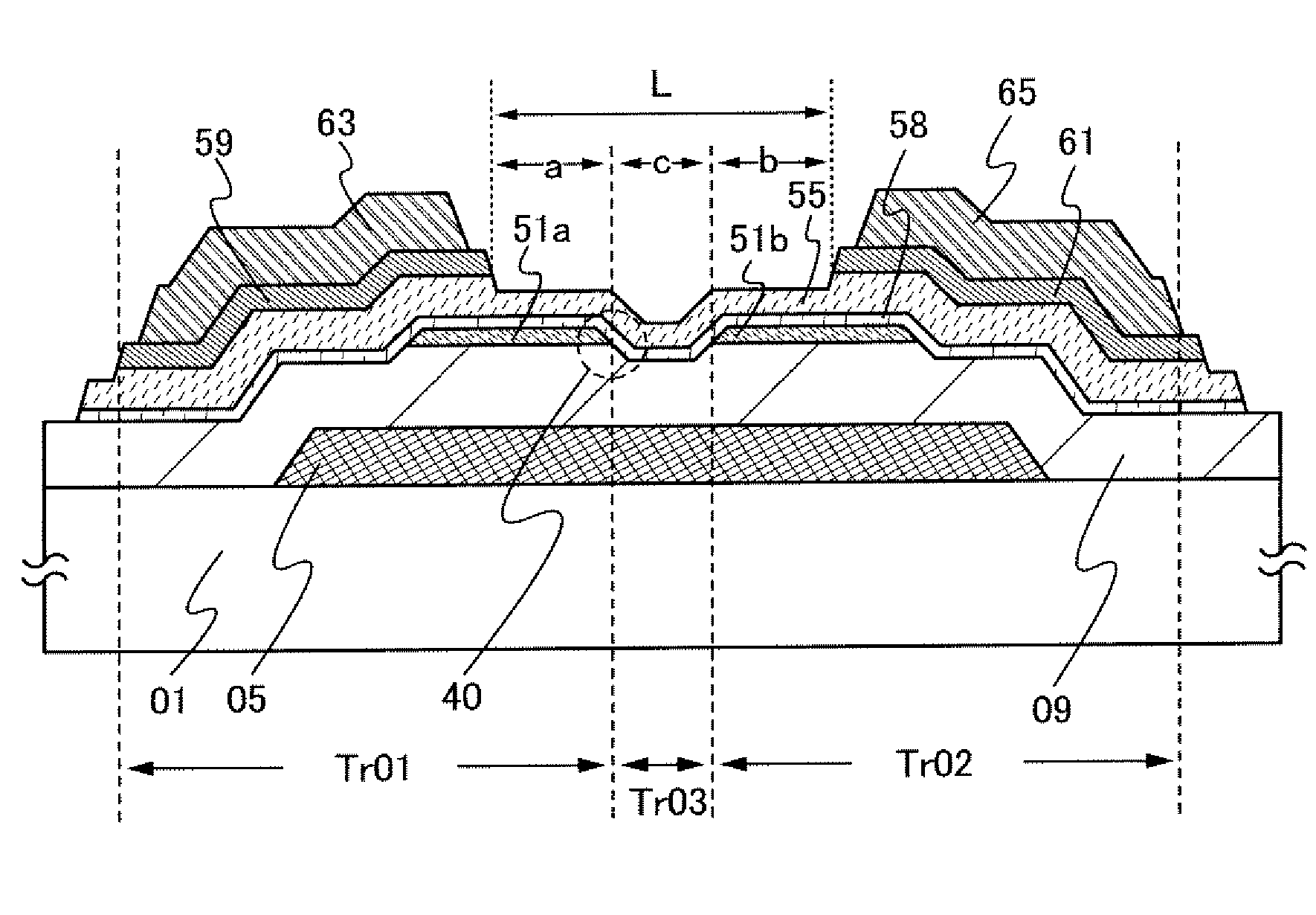
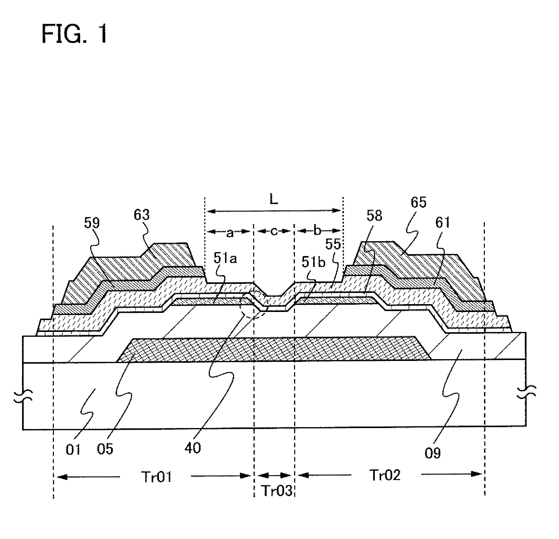
[0053]Here, a structure of a thin film transistor is described with reference to FIG. 1, which has smaller off-state current than a thin film transistor having a microcrystalline semiconductor layer in a channel formation region and which is capable of operating at higher speed and has larger on-state current than a thin film transistor having an amorphous semiconductor layer in a channel formation region.

[0054]In a thin film transistor illustrated in FIG. 1, a gate electrode 05 is formed over a substrate 01; a gate insulating layer 09 is formed over the gate electrode 05; first microcrystalline semiconductor layers 51a and 51b which are separated from each other are formed over the gate insulating layer 09; and a second microcrystalline semiconductor layer 58 is formed over the first microcrystalline semiconductor layers 51a and 51b and the gate insulating layer 09 In addition, an amorphous semiconductor layer 55 is formed to cover the second microcrystalline semiconductor layer 58...

embodiment mode 2

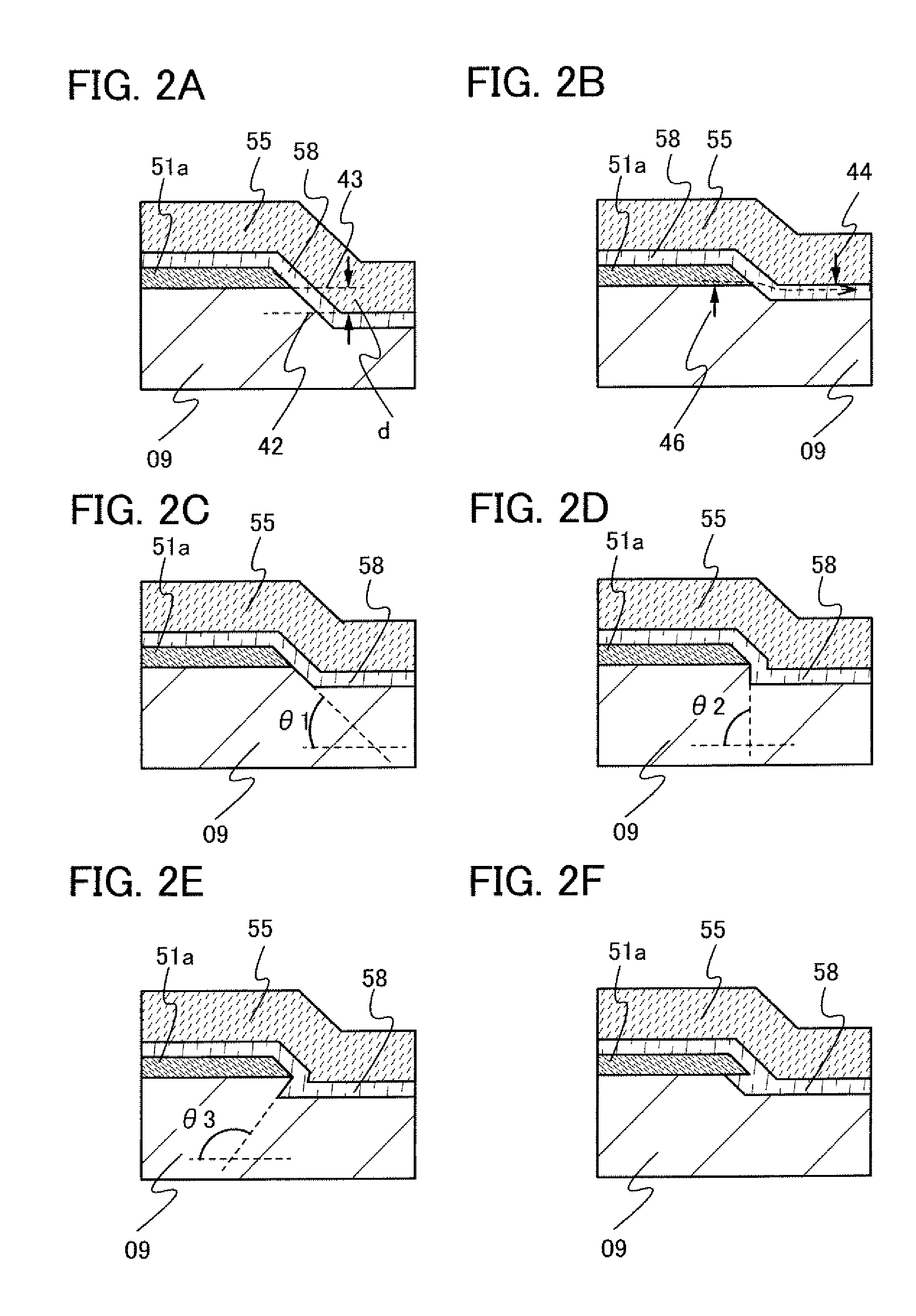
[0100]In this embodiment mode, a structure of a thin film transistor with still larger on-state current and higher field-effect mobility than those in Embodiment Mode 1 is described with reference to FIG. 4. In addition, a structure of a TFT with which off-state current can be reduced is described.

[0101]A thin film transistor described in this embodiment mode differs from the thin film transistor described in Embodiment Mode 1, in that buffer layers 53a and 53b are provided between the first microcrystalline semiconductor layers 51a and 51c and the second microcrystalline semiconductor layer 58. The buffer layers 53a and 53b are provided so as to roughly overlap the first microcrystalline semiconductor layers 51a and 51b.

[0102]The buffer layers 53a and 53b are formed using an amorphous semiconductor layer. The buffer layers 53a and 53b are preferably formed using an i-type or a substantially i-type amorphous semiconductor layer. Alternatively, an amorphous semiconductor layer to wh...

embodiment mode 3

[0107]In this embodiment mode, another embodiment of the second microcrystalline semiconductor layer is described with reference to FIG. 5. A feature of this embodiment mode is that two second microcrystalline semiconductor layers are provided, one of which, on the side in contact with the gate insulating layer 09 and the first microcrystalline semiconductor layers 51a and 51b, is an i-type microcrystalline semiconductor layer or amorphous semiconductor layer and the other, on the side in contact with the amorphous semiconductor layer 55, is an n-type microcrystalline semiconductor layer or amorphous semiconductor layer.

[0108]In a thin film transistor illustrated in FIG. 5, a gate electrode 05 is formed over a substrate 01, a gate insulating layer 09 is formed over the gate electrode 05, and first microcrystalline semiconductor layers 51a and 51b which are separated from each other are formed over the gate insulating layer 09. An i-type semiconductor layer 58a is formed over the fir...


PUM


Abstract

A thin film transistor is provided, which includes a gate insulating layer covering a gate electrode, a microcrystalline semiconductor layer provided over the gate insulating layer, an amorphous semiconductor layer overlapping the microcrystalline semiconductor layer and the gate insulating layer, and a pair of impurity semiconductor layers which are provided over the amorphous semiconductor layer and to which an impurity element imparting one conductivity type is added to form a source region and a drain region. The gate insulating layer has a step adjacent to a portion in contact with an end portion of the microcrystalline semiconductor layer. A second thickness of the gate insulating layer in a portion outside the microcrystalline semiconductor layer is smaller than a first thickness thereof in a portion in contact with the microcrystalline semiconductor layer.

Description

BACKGROUND OF THE INVENTION[0001]1. Field of the Invention[0002]The present invention relates to a thin film transistor and a display device which operates using the thin film transistor.[0003]2. Description of the Related Art[0004]As one type of field-effect transistor, a thin film transistor whose channel region is formed using a semiconductor layer that is formed over a substrate having an insulating surface is known. Techniques for using amorphous silicon, microcrystalline silicon, and polycrystalline silicon for semiconductor layers in thin film transistors have been disclosed (see References 1 to 5). A typical application of thin film transistors is a liquid crystal display television device, in which thin film transistors have been put to practical use as a switching transistor for each pixel that constitutes a display screen.[0005][Reference 1] Japanese Published Patent Application No. 2001-053283[0006][Reference 2] Japanese Published Patent Application No. H5-129608[0007][R...

Claims


Application Information

Patent Timeline
Patent Type & Authority Applications(United States)
IPC IPC(8): H01L29/04
CPCH01L29/04H01L29/78696H01L29/66765
Inventor YAMAZAKI, SHUNPEIKUROKAWA, YOSHIYUKIGODO, HIROMICHIMIYAIRI, HIDEKAZU
Owner SEMICON ENERGY LAB CO LTD
Why Eureka
Try Eureka