Component built-in wiring board

a built-in wiring and component technology, applied in the direction of fixed capacitor details, fixed capacitors, printed circuit non-printed electric components association, etc., can solve the problems of hard to directly connect the ic chip onto the mother board, hard to embed a capacitor in the core substrate, and the inability to reliably reduce the switching noise of the ic chip by the capacitor, etc., to achieve the effect of reducing thickness, reducing density, and reducing siz

Active Publication Date: 2009-09-24
NGK SPARK PLUG CO LTD
View PDF38 Cites 76 Cited by
  • Summary
  • Abstract
  • Description
  • Claims
  • Application Information

AI Technical Summary

Benefits of technology

[0022]Although the electrode layer or the dielectric layer in the capacitor may be constituted by only one layer or may be constituted by two layers or more, it is advantageous that the number of the electrode layers or the dielectric layers should be small. If the number of the electrode layers or the dielectric layers is increased, it is impossible to increase the density and to reduce the size (to reduce a thickness) in the component built-in wiring board while it is possible to increase a capacity of the capacitor. In this case, therefore, it is advantageous that an external dimension of the capacitor should be set to be larger than that of the first component and that of the component mounting region, and a region in which the capacitor is provided should include a region in which the first component is provided and the component mounting region when viewed from the thickness direction of the component built-in wiring board. Also, when the thickness of the component built-in wiring board is reduced, consequently, it is possible to increase the capacity of the capacitor by setting the external dimension of the capacitor to be large.
[0023]For example, material for forming the electrode layer may include silver, gold, platinum, copper, titanium, aluminum, palladium, nickel and tungsten. In particular, it is advantageous to use the nickel having a comparatively high melting point. In this case, if the dielectric layer is formed by ceramic having a high dielectric constant, it can be simultaneously burnt together with the dielectric layer. Moreover, the electrode layer is formed of comparatively inexpensive material. Therefore, it is possible to reduce a cost of the capacitor.
[0024]It is advantageous that the thickness of the electrode layer should be equal to or greater than 0.1 μm and should be equal to or smaller than 50 μm, for example. If the thickness of the electrode layer is smaller than 0.1 μm, there is a possibility that the electrical reliability might be ensured with difficulty. On the other hand, if the thickness of the electrode layer is greater than 50 μm, there is a possibility that the thickness of the whole capacitor might be increased. If the thickness is set in a range of 0.1 μm or more to 50 μm or less, it is possible to prevent an increase in the thickness of the whole capacitor while ensuring the electrical reliability.

Problems solved by technology

For this reason, it is hard to directly connect the IC chip onto the mother board.
Therefore, it is hard to embed a capacitor in the core substrate.
Consequently, it is impossible to reliably reduce a switching noise of the IC chip by the capacitor and to surely stabilize a power voltage.

Method used


Image

  • Component built-in wiring board
  • Component built-in wiring board
  • Component built-in wiring board

Examples


Embodiment Construction

[0048]Exemplary embodiments of the present invention will be now described with reference to the drawings.

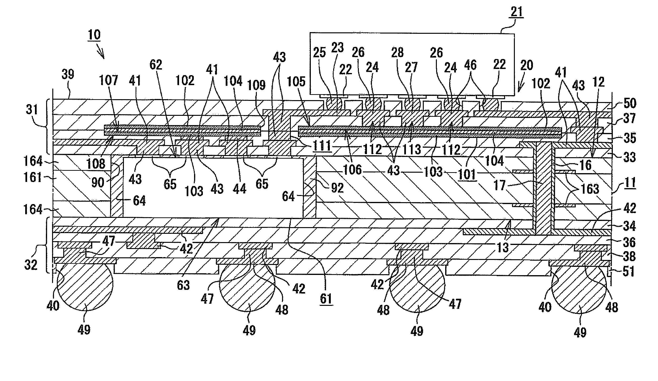
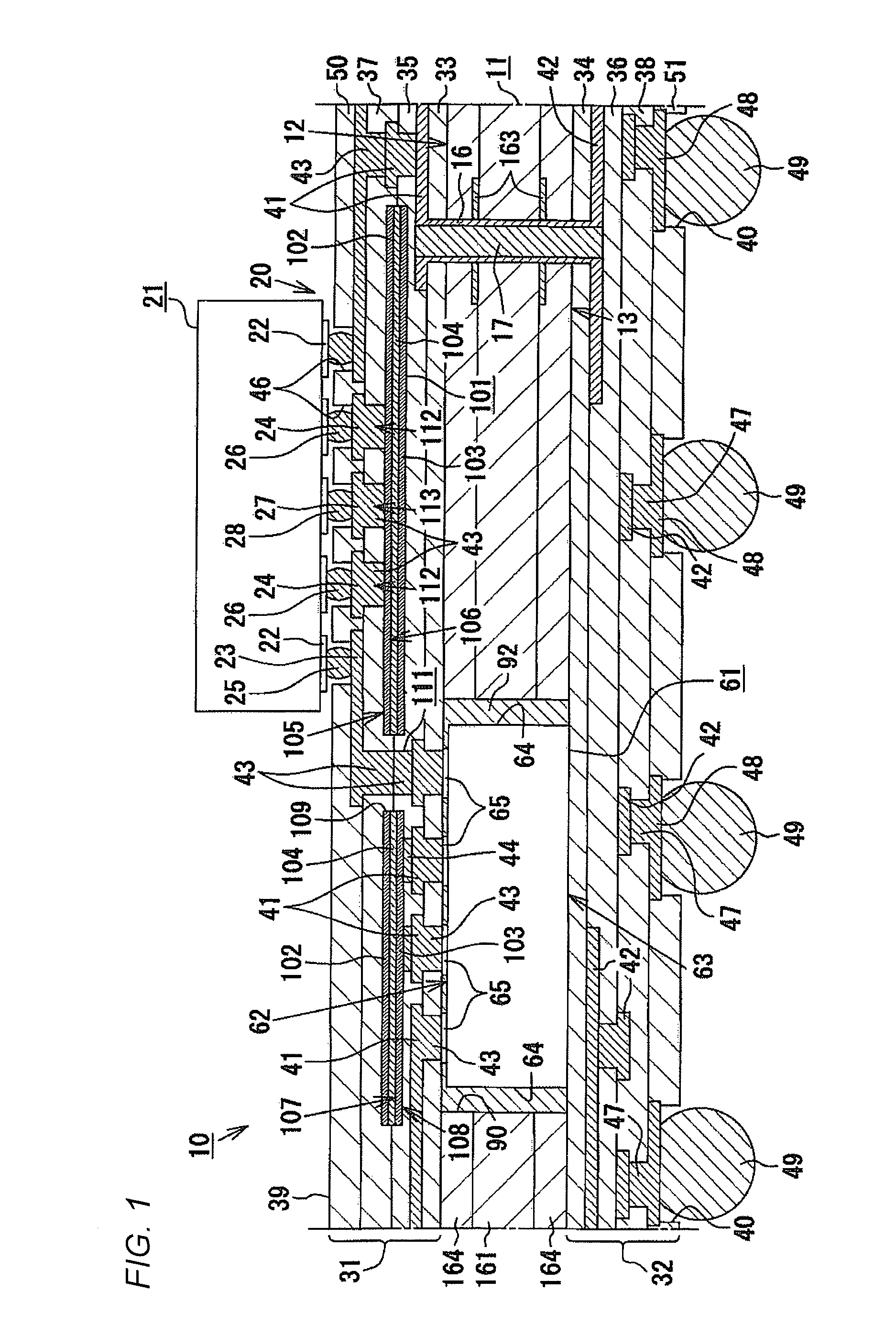
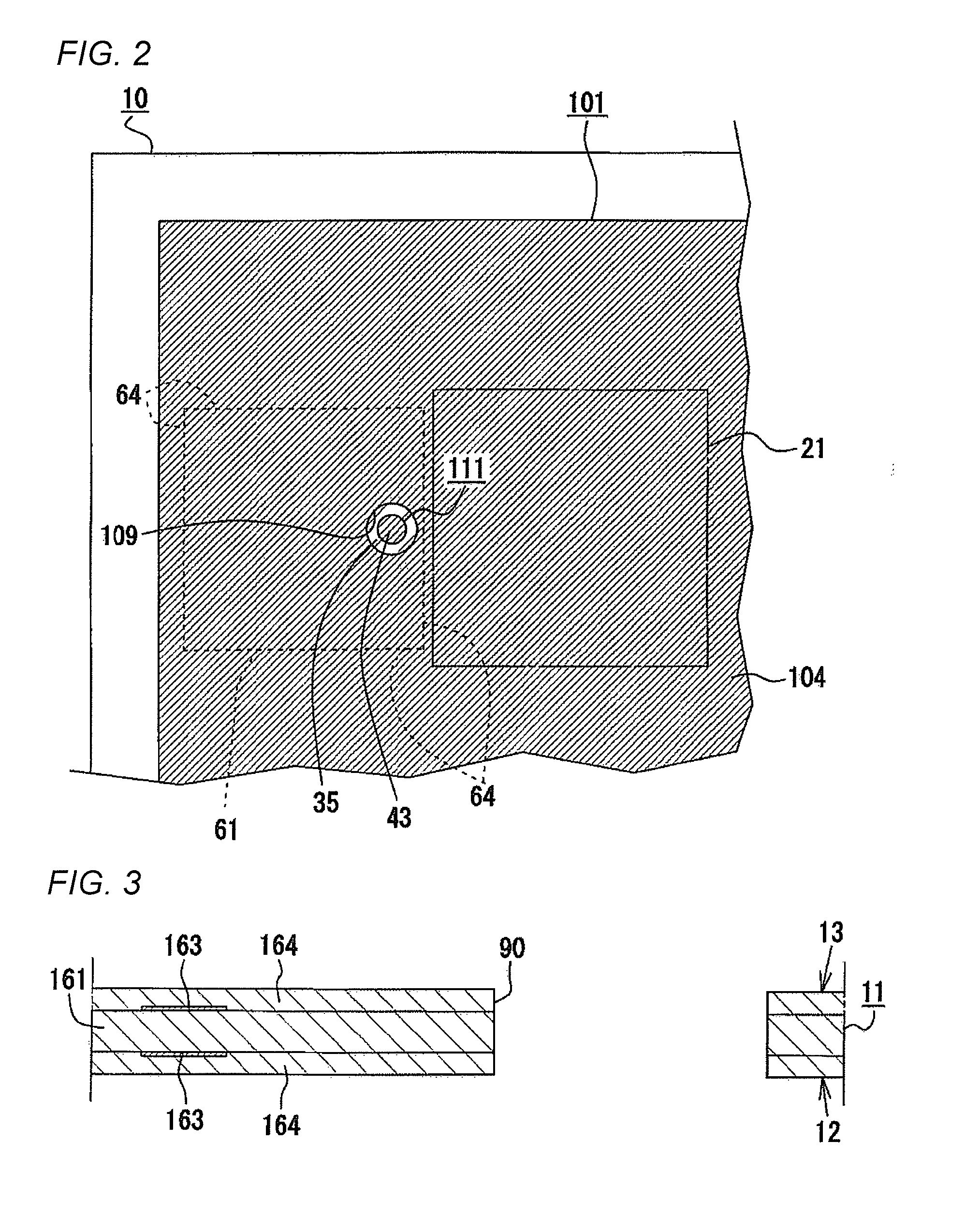
[0049]As shown in FIG. 1, a component built-in wiring board according to the exemplary embodiment (which will be hereinafter referred to as a “wiring board”) 10 is a wiring board for integrating an IC chip. The wiring board 10 is constituted by a core substrate 11 having a shape of an almost rectangular plate, a first built-up layer 31 formed on a core front surface 12 (an upper surface in FIG. 1) of the core substrate 11, and a second built-up layer 32 formed on a core back surface 13 (a lower surface in FIG. 1) of the core substrate 11.

[0050]The core substrate 11 according to the exemplary embodiment has a shape of an almost rectangular plate seen on a plane in a length of 25 mm, a width of 25 mm and a thickness of 1.0 mm. The core substrate 11 has a coefficient of thermal expansion in a planar direction (an XY direction) which is approximately 10 to 30 ppm / ° C. (more specific...


PUM


Abstract

A component built-in wiring board is provided. The component built-in wiring board 10 includes a core substrate 11, a first component 61, a first built-up layer 31 and a capacitor 101. The core substrate 11 has a housing hole 90 and the first component 61 is housed in the housing hole 90. A component mounting region 20 capable of mounting a second component 21 is provided in a surface 39 of the first built-up layer 31. The capacitor 101 has electrode layers 102 and 103 and a dielectric layer 104. The capacitor 101 is embedded in the first built-up layer 31 such that a first front surface 105 and a second front surface 106 in the electrode layer 102 and a first front surface 107 and a second front surface 108 in the electrode layer 103 are disposed in parallel with the surface 39 of the first built-up layer 31.

Description

CROSS-REFERENCE TO RELATED APPLICATIONS[0001]This application claims priority from Japanese Patent Application No. 2008-075169, filed on Mar. 24, 2008, the entire contents of which are hereby incorporated by reference.BACKGROUND OF THE INVENTION[0002]1. Technical Field[0003]Devices consistent with the present invention relate to a component built-in wiring board which includes a capacitor having an electrode layer and a dielectric layer.[0004]2. Related Art[0005]In recent years, a semiconductor integrated circuit device (an IC chip) to be used as a microprocessor of a computer has been enhanced in a speed and a function increasingly. Incidentally, there is a tendency that the number of terminals is increased and a pitch between the terminals is also reduced. In general, a large number of terminals are densely disposed in an array on a bottom surface of the IC chip, and the terminal group is connected to a terminal group on a mother board side by flip chip bonding. The pitch between ...

Claims


Application Information

Patent Timeline
Patent Type & Authority Applications(United States)
IPC IPC(8): H05K1/18
CPCH01L23/49838H01L23/50H01L2924/1461H01L2224/16225H01L2924/01047H01L2924/01033H01L2924/01006H01L23/5389H01L24/24H01L24/82H01L2224/24227H01L2224/82039H01L2224/82047H01L2924/01009H01L2924/01013H01L2924/01027H01L2924/01029H01L2924/01038H01L2924/01046H01L2924/01056H01L2924/01074H01L2924/01078H01L2924/01079H01L2924/01082H01L2924/14H01L2924/15153H01L2924/1517H01L2924/15311H01L2924/19041H01L2924/19043H01L2924/30105H01L2924/30107H05K1/162H05K1/185H05K3/4602H05K2201/09309H05K2201/09509H05K2201/09718H05K2201/10674H01L2924/00H01L24/19H01L24/20H01L2224/02377H01L2224/02379H01L2224/04105H01L2224/05001H01L2224/05024H01L2224/05026H01L2224/05027H01L2224/05147H01L2224/05548H01L2224/05568H01L2224/06131H01L2224/12105H01L2224/73267H01L2924/00014
Inventor ORIGUCHI, MAKOTOTAKASHIMA, TSUNEAKI
Owner NGK SPARK PLUG CO LTD
Why Eureka
Try Eureka