Transmission electron microscope having electron spectroscope

a technology of electron microscope and electron spectrometer, which is applied in the field of transmission electron microscope having an electron spectroscope, can solve the problems of difficult to completely match the shapes, positions and the like of the zero loss spectra or completely match, complicated adjustment of lenses, and long adjustment time of plurality of lenses, etc., to achieve high efficiency, high accuracy, and high efficiency

Active Publication Date: 2009-10-01
HITACHI HIGH-TECH CORP
View PDF3 Cites 16 Cited by
  • Summary
  • Abstract
  • Description
  • Claims
  • Application Information

AI Technical Summary

Benefits of technology

[0024]According to the present invention, the standard spectral image such as a zero loss spectral image or an electron energy loss spectral image acquired from a reference sample made of a single type of composition is acquired; an electron energy loss spectral image is acquired from the sample to be analyzed; and the electron energy loss spectral image acquired from the sample to be analyzed is corrected based on the difference between the spectrum extracted from the standard portion of the standard spectral image and the spectrum extracted from each of the measured portions that are different from the standard portion and included in the standard spectral image. The electron energy loss spectral image is a two-dimensional image having two parameters indicative of the amount of an energy loss and positional information on the sample. The transmission electron microscope having the electron spectroscope is capable of correcting, with high efficiency an

Problems solved by technology

It is, however, difficult to completely match the shapes, positions and the like of the zero loss spectra or completely match the shapes, positions and the like of the electron energy loss spectra acquired from the sample made of a single t

Method used


Image

  • Transmission electron microscope having electron spectroscope
  • Transmission electron microscope having electron spectroscope
  • Transmission electron microscope having electron spectroscope

Examples


embodiment

[0038]An embodiment of the present invention is described below with reference to the accompanying drawings. In all of the accompanying drawings used to explain the embodiment, the same elements are denoted by the same reference numerals in principle, and duplicate description is omitted.

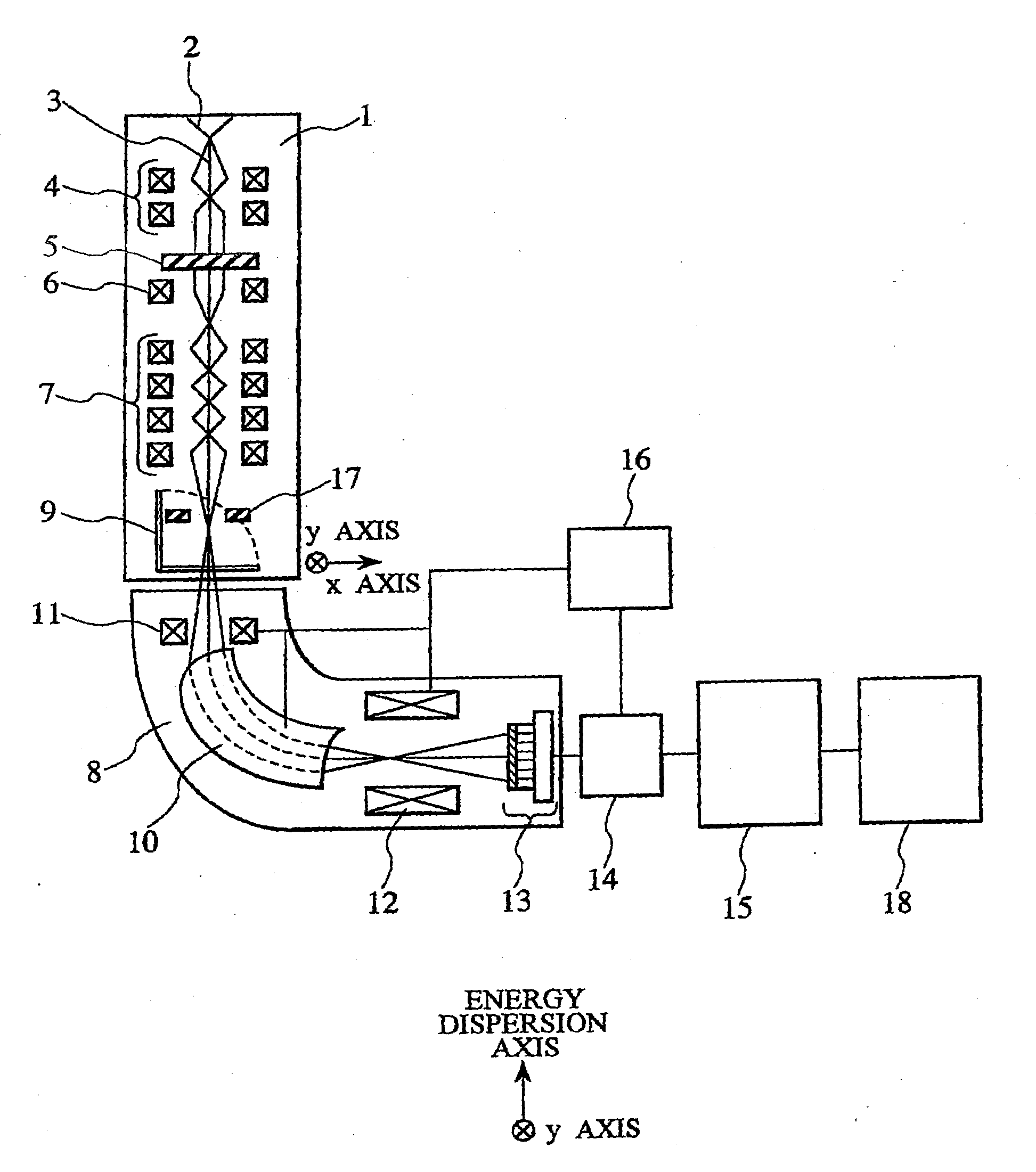
[0039]FIG. 1 is an outline diagram showing an example of the configuration of a transmission electron microscope having an electron spectroscope according to an embodiment of the present invention.

[0040]The transmission electron microscope according to the embodiment is provided with the electron spectroscope and has a transmission electron microscope 1, an electron spectroscope 8, an image display unit 14, a central control unit 16, a spectrum correction system 15 and the like. The transmission electron microscope 1 includes an electron source 2, a convergent lens 4, an objective lens 6, an imaging lens system 7, and a fluorescent plate 9. A sample 5 is placed between the convergent lens 4 and the ...


PUM


Abstract

A transmission electron microscope is capable of correcting, with high efficiency and high accuracy, an electron energy loss spectrum extracted from each of measured portions included in an electron energy loss spectral image with two axes representing the amount of an energy loss and positional information on a measured portion. The transmission electron microscope has an electron spectroscope and a spectrum correction system. The spectrum correction system corrects a spectrum extracted from each measured portion included in an electron energy loss spectral image acquired from a sample based on a difference between a spectrum extracted from a standard portion of a standard spectral image and a spectrum extracted from a portion different from the standard portion.

Description

BACKGROUND OF THE INVENTION[0001]1. Field of the Invention[0002]The present invention relates to a transmission electron microscope having an electron spectroscope that spectrally decomposes an electron beam based on the amount of energy of the electron beam.[0003]2. Description of the Related Art[0004]The sizes of processed silicon semiconductors, the sizes of processed magnetic devices and the like have become minute. Thus, a reduction in degradation of characteristics of devices and a reduction in reliability of the devices are critical issues. In recent years, a two-dimensional element analysis, a spectral analysis using (scanning) transmission electron microscopy ((S)TEM) and a spectral analysis using electron energy loss spectroscopy (EELS) have been required in order to analyze a defect of a nanometer-sized area of a semiconductor device, and find and solve the cause of the defect in a new process for developing a device and in a new process for mass production.[0005]An elect...

Claims


Application Information

Patent Timeline
IPC IPC(8): G01N23/00G01D18/00
CPCG01N23/04G01N2223/3037G01N2223/102
Inventor TERADA, SHOHEITANIGUCHI, YOSHIFUMI
Owner HITACHI HIGH-TECH CORP
Why Eureka
Try Eureka