Pulse-Laser Bonding Method for Through-Silicon-Via Based Stacking of Electronic Components

a technology of throughsilicon and bonding temperature, applied in the direction of basic electric elements, manufacturing tools, solid-state devices, etc., can solve the problems of high bonding temperature, difficult method implementation, and large in-plane size of wire bonding

Active Publication Date: 2009-10-01
HONG KONG APPLIED SCI & TECH RES INST
View PDF20 Cites 36 Cited by
  • Summary
  • Abstract
  • Description
  • Claims
  • Application Information

AI Technical Summary

Benefits of technology

[0018]In preferred embodiments of the invention the laser energy pulse is between 1 and 70 J. The laser energy pulse may have a duration of between 1 μs and 20 ms, more

Problems solved by technology

Traditionally wire bonding is used to establish electrical interconnect between chips, but wire-bonding requires greater in-plane size and is inconsistent with the objective of maximizing the component density.
Diffusion bonding produces a good quality bond that is reliable, but disadvantages of this method include the requirement for very good coplanarity of the two semiconductor components and the need for a high bonding temperature.
The method is therefore diffic

Method used


Image

  • Pulse-Laser Bonding Method for Through-Silicon-Via Based Stacking of Electronic Components
  • Pulse-Laser Bonding Method for Through-Silicon-Via Based Stacking of Electronic Components
  • Pulse-Laser Bonding Method for Through-Silicon-Via Based Stacking of Electronic Components

Examples


Embodiment Construction

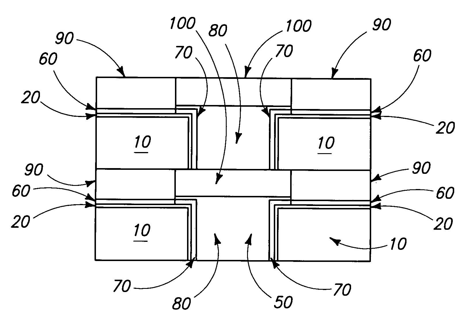
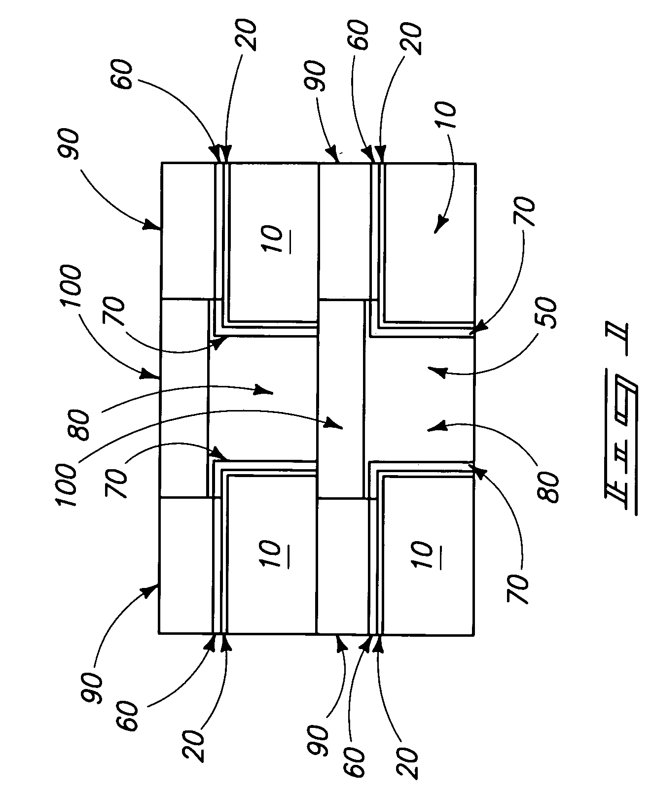
[0025]FIG. 1 shows a section through two silicon chips connected by means of through-silicon-vias formed in accordance with an embodiment of the invention. The via provides an electrical interconnection between two silicon chips 10. Each chip 10 is provided with an via hole 50 extending through the chip 10. The interior surface of each via hole is finished with an adhesion layer 70 (for example formed of TiW alloy, Cr, or Ti), and an isolation layer 20 (for example formed of SiO2) that is also provided on the upper surface of each chip. The space between the two chips 10 is filled with a polymer bonding material 90. Suitable materials for the polymer material 90 include polyimide (PI), benzocyclobytene (BCB), epoxy, a non-conductive adhesive, or silicon rubber.

[0026]Each via hole through the chips 10 is filled with metal (e.g., copper, gold, tin, indium, silver, nickel, solders) to form a metal plug that adheres to the adhesion layer 70. Between the plugs that fill the respective vi...


PUM

PropertyMeasurementUnit
Timeaaaaaaaaaa
Timeaaaaaaaaaa
Timeaaaaaaaaaa

Abstract

There is described a method of forming a through-silicon-via to form an interconnect between two stacked semiconductor components using pulsed laser energy. A hole is formed in each component, and each hole is filled with a plug formed of a first metal. One component is then stacked on another component such that the holes are in alignment, and a pulse of laser energy is applied to form a bond between the metal plugs.

Description

FIELD OF THE INVENTION[0001]This invention relates to a pulse-laser based bonding method for through-silicon-via (TSV) based 3D die-stacking.BACKGROUND OF THE INVENTION[0002]With electronic devices, particularly portable devices such as mobile phones, becoming smaller and yet at the same time offering a wider range of functions, there is a need to integrate multifunctional chips but without increasing the size of the devices and keeping a small form factor. Increasing the number of electronic components in a 2D structure is incompatible with these objectives, and therefore 3D packages are increasingly being adopted in order to provide greater functionality and higher component density but with a small form factor.[0003]In a 3D structure electronic components such as semiconductor chips may be provided in a multilayer stacked structure. To connect electrically the components in different layers through-silicon-via (TSV) technology may be used to provide the electrical interconnect an...

Claims


Application Information

Patent Timeline
IPC IPC(8): H01L23/538B23K26/22H01L21/44
CPCH01L21/6835H01L21/76898H01L2924/0002H01L2924/07802H01L2224/0401H01L2224/8182H01L2924/10253H01L24/27H01L2224/29101H01L2924/0665H01L2924/014H01L2924/01076H01L2924/01074H01L2924/01073H01L2924/01033H01L24/13H01L24/29H01L24/81H01L24/94H01L25/0657H01L25/50H01L2221/68359H01L2224/0557H01L2224/13099H01L2224/16H01L2224/274H01L2225/06513H01L2225/06541H01L2924/01022H01L2924/01029H01L2924/01046H01L2924/01047H01L2924/01049H01L2924/0105H01L2924/0106H01L2924/01078H01L2924/01079H01L2924/01082H01L2924/01327H01L2924/04941H01L2224/2919H01L2924/01005H01L2924/01006H01L2924/01024H01L2924/00H01L2224/05552H01L2924/351H01L2224/05166H01L2224/05171H01L2224/05611H01L2224/05639H01L2224/05644H01L2224/05647H01L2224/05655H01L2224/056H01L2224/16146H01L24/11H01L24/05H01L24/03H01L2224/13025H01L2924/00014H01L2924/013
Inventor SHI, XUNQINGMA, WEIXIE, BINCHUNG, CHANG HWA
Owner HONG KONG APPLIED SCI & TECH RES INST
Why Eureka
Try Eureka