Active solid heatsink device and fabricating method thereof

Active Publication Date: 2009-10-01
IND TECH RES INST
View PDF5 Cites 7 Cited by
  • Summary
  • Abstract
  • Description
  • Claims
  • Application Information

AI Technical Summary

Benefits of technology

[0014]An insulating layer can be covered on the other side of the metal layer opposite to the first substrate, so as to serve as a substrate which is shared by the TE structure during subsequent processing. Then, at least one TE element can be formed on the insulating layer, and a second substrate is connected to the other end of the TE element opposite to the insulating layer. In this manner, the heat energy spreading to the insulating layer can be pumped to the second substrate by the TE, so as to further improve the heat dissipation efficiency.

Problems solved by technology

When an electron industry process is improved from 90 nm to 65 nm or even 45 nm, the heat generation of a developed “multi-core” integrated circuit (IC) has been reduced from 130 W (watt) to 80 W. In this manner, although the high heat generation problem has been solved, the problem of hot spots occurs on an IC chip.
At the same time, the generation of the hot spots will lower the performance of the IC chip (e.g. a processor).
Although a conventional heatsink device (e.g. air cooled type or air cooled type used in conjunction with the heat pipes) can settle down the problem of the total heat generation of the processor, the hot spots cannot be effectively eliminated.
Therefore, the heat dissipation problem of the LEDs is also a technical bottleneck to be solved by the photoelectric semiconductor industry.
Thus, the heat dissipation effect is poor.
Due to the physical limitations, the conventional TI element cannot achieve the cooling requirements under the normal temperature.
However, in the conventional active solid heatsink device, a single pin area is larger than or equal to the area of the hot spot, and the high heat-generating density of the hot spot exceeds a heat load of a single pin.
Therefore, the effect of merely using the active solid heatsink device for eliminating the hot spots is quite limited.

Method used


Image

  • Active solid heatsink device and fabricating method thereof
  • Active solid heatsink device and fabricating method thereof
  • Active solid heatsink device and fabricating method thereof

Examples


Embodiment Construction

[0042]FIGS. 1A to 1C show a method of fabricating an active solid heatsink device according to an embodiment of the present invention.

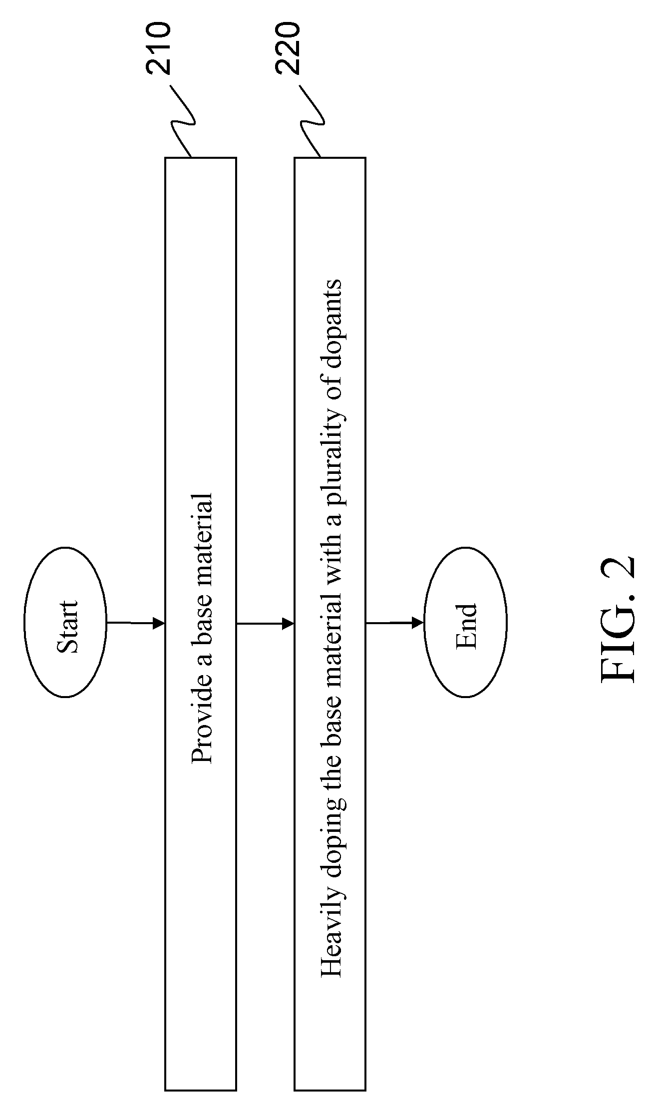
[0043]A heavy doped first substrate 110 is provided, a shown in FIG. 1A. The heavy doped first substrate 110 can be obtained through the following steps. Referring to FIG. 2, first, the base material for fabricating the first substrate 110 is provided (step 210). Then, the base material is heavily doped with a plurality of dopants (step 220), so as to obtain the first substrate 110 as shown in FIG. 1A. For example, the first substrate 110 can be, but not limited to, heavy doped P or N silicon substrate.

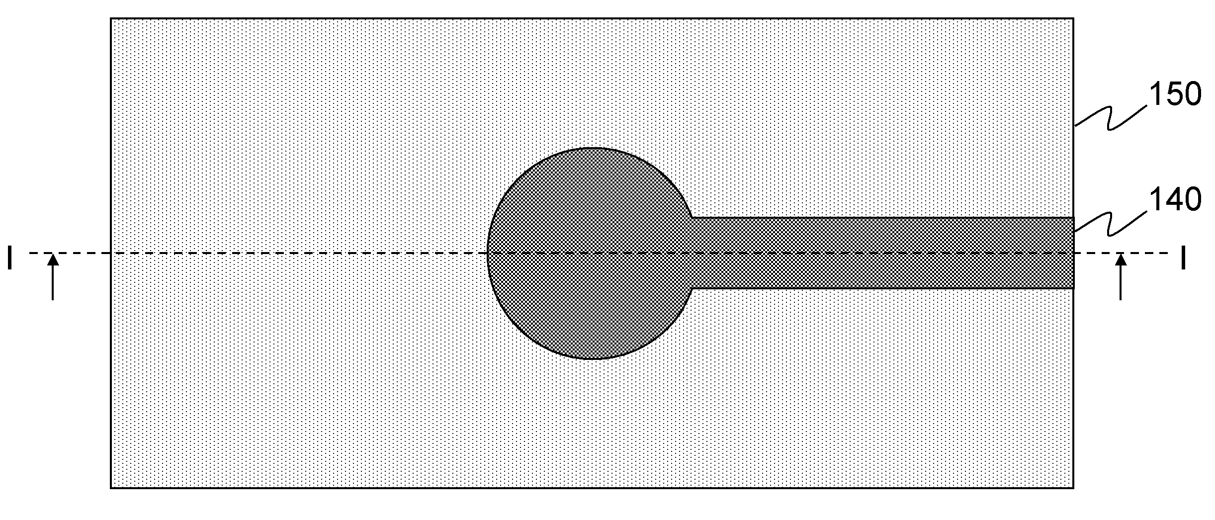
[0044]A semiconductor film block (e.g. a super lattice barrier 130 for convenience of illustration) and a metal layer 150 are formed on the same surface of the first substrate 110, as shown in FIGS. 1B and 3. The super lattice barrier 130 and the metal layer 150 are spaced apart. In addition to a column as shown in the figure, the super lattice barrier ...


PUM


Abstract

An active solid heatsink device and fabricating method thereof is related to a high-effective solid cooling device, where heat generated by a heat source with a small area and a high heat-generating density diffuses to a whole substrate using a heat conduction characteristic of hot electrons of a thermionic (TI) structure, and the thermionic (TI) structure and a thermo-electric (TE) structure share the substrate where the heat diffuses to. Further, the shared substrate serves as a cold end of the TE structure, and the heat diffusing to the shared substrate is pumped to another substrate of the TE structure serving as a hot end of the TE structure.

Description

CROSS-REFERENCE TO RELATED APPLICATIONS[0001]This non-provisional application claims priority under 35 U.S.C. §119(a) on Patent Application No(s). 097111577 filed in Taiwan, R.O.C. on Mar. 28, 2008 the entire contents of which are hereby incorporated by reference.BACKGROUND[0002]1. Field of Invention[0003]The present invention relates to a heatsink device, and more particularly to an active solid heatsink device and fabricating method thereof.[0004]2. Related Art[0005]When an electron industry process is improved from 90 nm to 65 nm or even 45 nm, the heat generation of a developed “multi-core” integrated circuit (IC) has been reduced from 130 W (watt) to 80 W. In this manner, although the high heat generation problem has been solved, the problem of hot spots occurs on an IC chip. A so-called hot spot is a local heat-generating portion with an area of approximately 50 μm (micrometer)*50 μm. On the hot spots, a local heat flux can be up to 150 W / cm2 to 1000 W / cm2. At the same time, t...

Claims


Application Information

Patent Timeline
IPC IPC(8): H01L23/34H01S5/024
CPCH01L23/38H01L27/16H01S3/04H01S5/024H01L2924/0002H01S5/02476H01L2924/00H10N19/00
Inventor YU, CHIH-KUANGLIU, CHUN-KAIDAI, MING-JICHENG, CHIH-YUAN
Owner IND TECH RES INST
Why Eureka
Try Eureka