Trench monos memory cell and array
a monos memory and array technology, applied in the field of monos memory storage devices, can solve the problems of difficult neutralization of electrons stored over the middle of the channel, difficulty in program-erase cycle vt shift, and difficulty in reducing the threshold voltage (vt) of the nrom structure, so as to prevent read disturbance and high concentration
- Summary
- Abstract
- Description
- Claims
- Application Information
AI Technical Summary
Benefits of technology
Problems solved by technology
Method used
Image

Examples
first embodiment
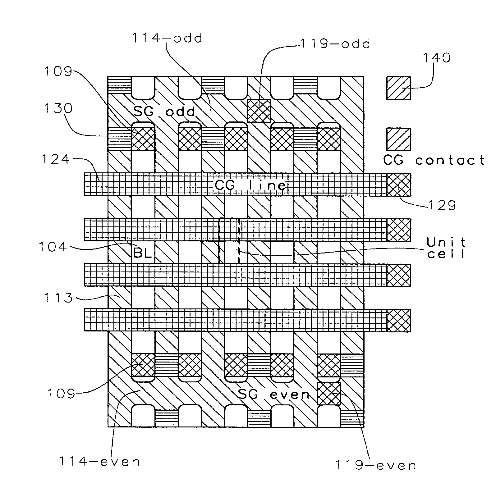
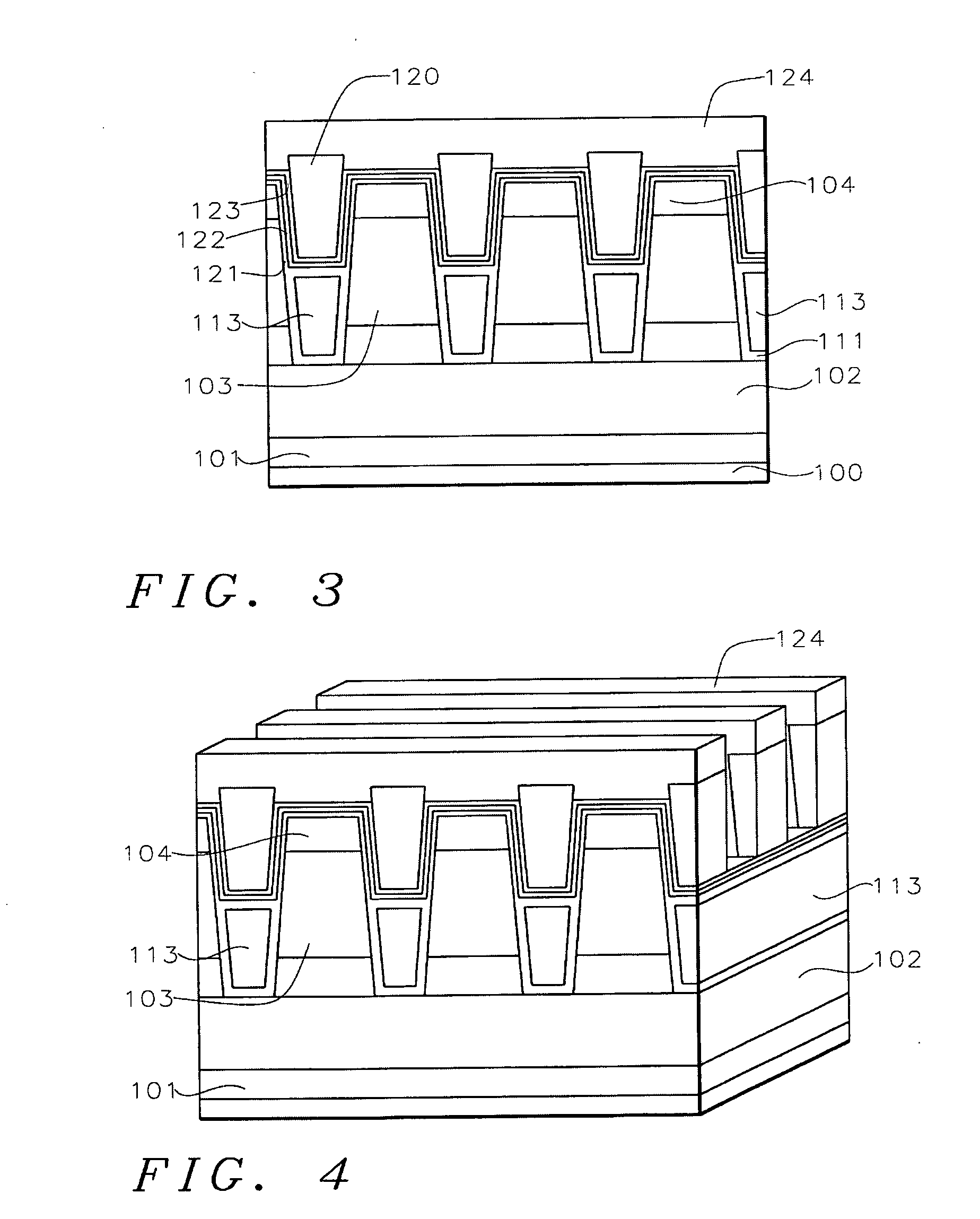
[0033]The cross-sectional memory structure of the invention is shown in FIG. 3. The vertical channel is in the p-region 103 between top 104 and bottom 102 n-regions along a trench split gate pair of a control gate 120 and select gate 113. A bottom part of the split gate is used to select an odd or even column. The select gate consists of a gate electrode 113 and gate oxide 111 in between the channel and the gate electrode. A top part of the split gate pair is used to control device operations such as write, erase and read. The control gate consists of a gate electrode 120 and a stack of oxide 121 nitride 122 and oxide 123 in between the gate electrode and the vertical channel. Nitride layer 122 in the stack layer functions as a memory element. The stack layer is also in between the top gate electrode and the bottom gate electrode to separate the gates.
[0034]The bottom of the select gate is located deeper than the bottom p-n junction defined by the boundary of the n-region 102 and th...
second embodiment
[0044]The cross-sectional memory structure of the invention is shown in FIG. 13. The vertical channel is in the p-region 203 between top 216 and bottom 201 n-regions along a word gate 213. Insulation 209 under the word gate electrode separates the bottom n+ layer into two independent regions, odd 201-o and even 201-e. A stack layer of Oxide 210, Nitride 211 and oxide 212 is adapted as a word gate dielectric. Silicon Nitride layer 211 is a memory element. Memory storage is shown by 226. A bit line 217 connects top n+ regions 216 in a direction perpendicular to the word line.
[0045]A memory cell is selected by the word gate, odd or even bottom n+ region, and a bit line for read and program mode. Program is accomplished by injecting electrons into the nitride storage region located adjacent to the PN junction, where positive voltage is applied to a bit line and a word gate. A selected bottom n+ is grounded. Others are floated or disconnected. For read mode, a positive voltage is applied...
PUM
 Abstract
Description
Claims
Application Information
 - R&D
- Intellectual Property
- Life Sciences
- Materials
- Tech Scout
- Unparalleled Data Quality
- Higher Quality Content
- 60% Fewer Hallucinations
Browse by: Latest US Patents, China's latest patents, Technical Efficacy Thesaurus, Application Domain, Technology Topic, Popular Technical Reports.
© 2025 PatSnap. All rights reserved.Legal|Privacy policy|Modern Slavery Act Transparency Statement|Sitemap|About US| Contact US: help@patsnap.com