Semiconductor device and manufacturing method thereof

a technology of semiconductor devices and semiconductor devices, which is applied in the direction of semiconductor devices, diodes, electrical apparatus, etc., can solve the problems of deterioration in the reliability of semiconductor devices, difficult to cause characteristics variations of semiconductor devices, etc., and achieves low resistance, low on-resistance, and improved reliability

Active Publication Date: 2009-10-15
RENESAS ELECTRONICS CORP
View PDF7 Cites 44 Cited by
  • Summary
  • Abstract
  • Description
  • Claims
  • Application Information

AI Technical Summary

Benefits of technology

[0009]From the above description, it is apparent that the epitaxial layer functions as a current-flowing drift layer from the viewpoint of the power MISFET, while it functions as a semiconductor layer forming a Schottky junction from the viewpoint of the Schottky barrier diode. Since an electric current of the power MISFET passes through the epitaxial layer, it is therefore desired to have low resistance (low on-resistance).
[0010]The power MISFET and the Schottky barrier diode have been formed on one semiconductor substrate and both of these elements have an avalanche breakdown voltage. For example, the avalanche breakdown voltage of the power MISFET is determined by a pn junction between the epitaxial layer and the channel region. The avalanche breakdown voltage of the Schottky barrier diode is, on the other hand, determined by the doping concentration of the epitaxial layer which is a semiconductor layer forming a Schottky junction. From the standpoint of obtaining a semiconductor device having improved reliability, the avalanche breakdown voltage of the Schottky barrier diode is desirably higher than the avalanche breakdown voltage of the power MISFET.
[0013]An object of the invention is to provide a technology, in a semiconductor device having a power MISFET and a Schottky barrier diode on one semiconductor substrate, of making the avalanche breakdown voltage of the Schottky barrier diode higher than the avalanche breakdown voltage of the power MISFET, while suppressing a drastic increase in the on-resistance of the power MISFET.

Problems solved by technology

For example, when the avalanche breakdown voltage of the power MISFET is lower than the avalanche breakdown voltage of the Schottky barrier diode, breakdown occurs at the pn junction (between epitaxial layer and channel formation region) in the bulk, making it difficult to cause characteristics variations of the semiconductor device.
This means that characteristics variations have a greater influence on the entire semiconductor device when the avalanche breakdown occurs on the surface of the epitaxial layer than when the avalanche breakdown occurs inside the epitaxial layer, leading to deterioration in the reliability of the semiconductor device.

Method used


Image

  • Semiconductor device and manufacturing method thereof
  • Semiconductor device and manufacturing method thereof
  • Semiconductor device and manufacturing method thereof

Examples


embodiment 1

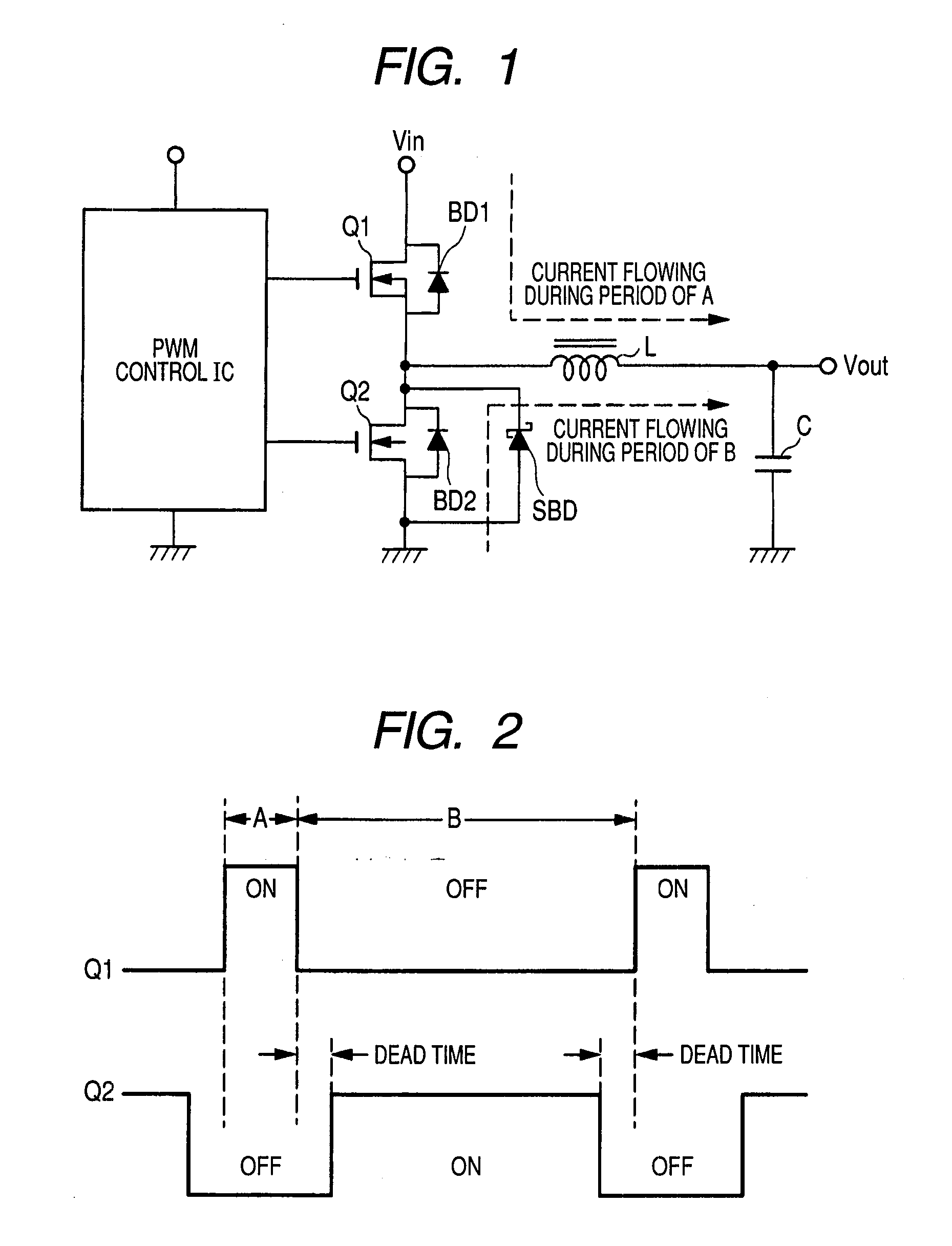
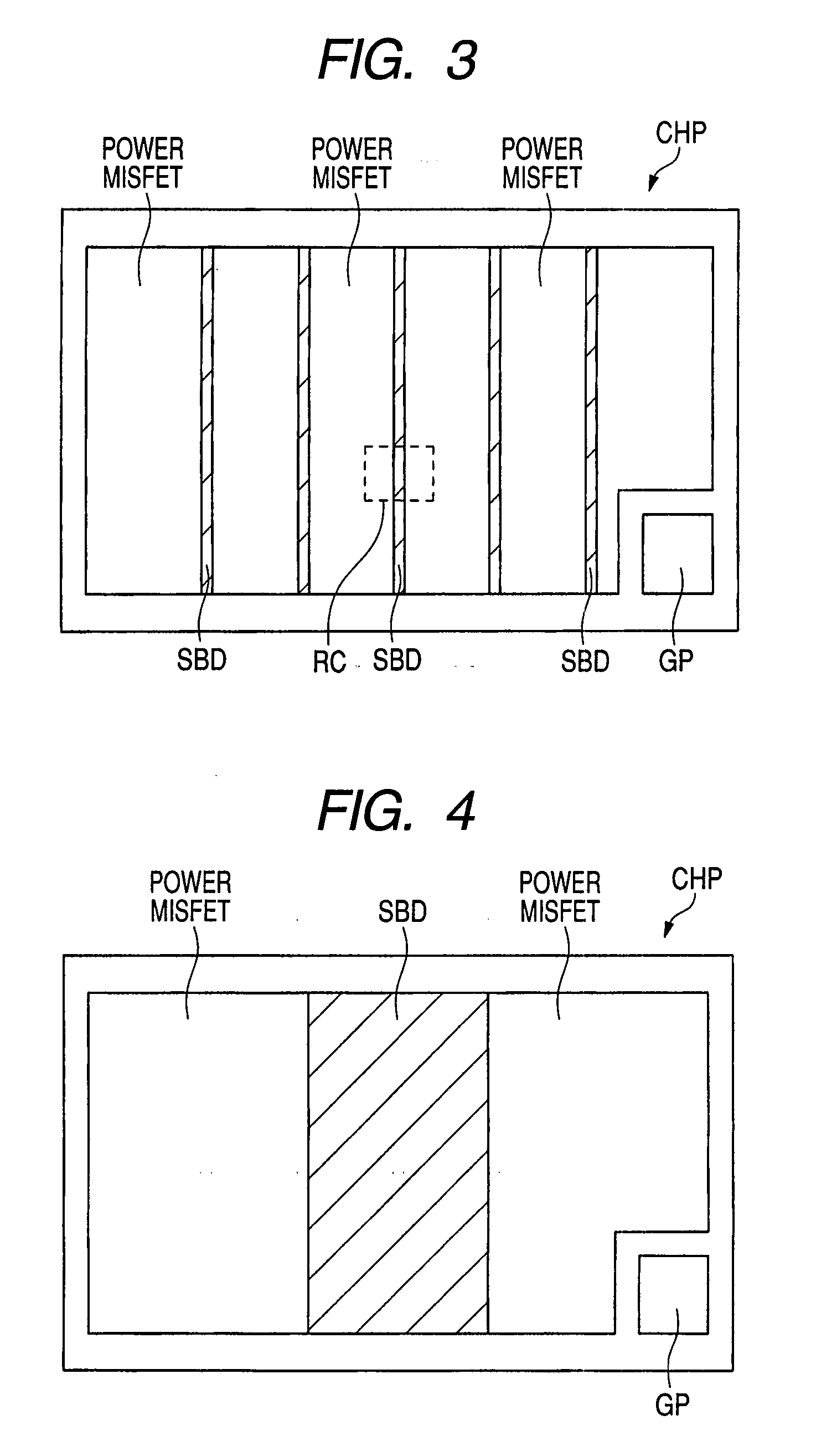
[0091]In Embodiment 1, two means are described as a means for adjusting the area of the Schottky barrier diode, that is, a means of forming a plurality of linear Schottky barrier diodes SBDs to increase the total area of the Schottky barrier diodes SBDs and a means of forming a thick and linear Schottky barrier diode SBD and widening this line width to increase the total area of the Schottky barrier diode SBD. It is also possible to use these two means in combination in order to adjust the area of the Schottky barrier diodes SBDs. Described specifically, a plurality of linear Schottky barrier diodes SBDs is formed and the width of each of the lines of the Schottky barrier diodes SBDs is increased, whereby the area of the Schottky barrier diodes SBDs can be adjusted.

[0092]In Patent Document 2, for example, the distance between trenches having a Schottky barrier diode SBR sandwiched therebetween is made narrower than the distance between trenches of cells in which a power MISFET has b...

embodiment 2

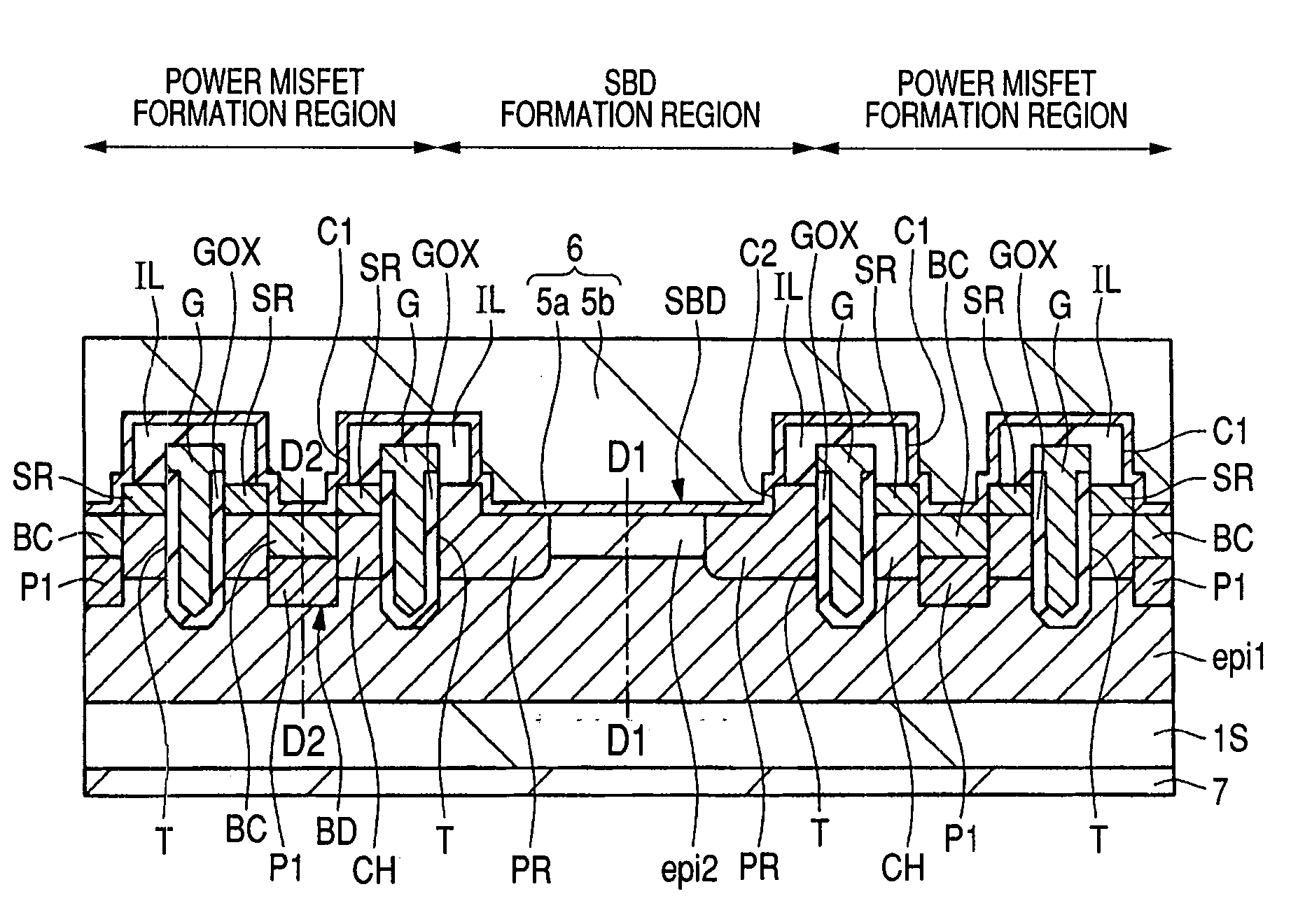
[0218]As illustrated in FIG. 45, also in Embodiment 2, a power MISFET and a Schottky barrier diode SBD are formed over the same semiconductor substrate 1S. The Schottky barrier diode SBD has a Schottky junction obtained by bringing an epitaxial layer epi2 having a low doping concentration into direct contact with a titanium tungsten film 5a configuring a first metal film 6. The Schottky barrier diode SBD is formed in a Schottky barrier diode SBD formation region. The p ring PR is formed in the end portions of the Schottky barrier diode SBD formation region so as to surround the Schottky barrier diode SBD with the p ring.

[0219]The p ring PR is arranged in such a manner because of the following reasons. For example, when the p ring PR is not formed, the epitaxial layer epi2 which is an n type semiconductor region is brought into direct contact with the trench T in the Schottky barrier diode SBD formation region. In this case, by a reverse bias voltage applied to the Schottky barrier d...


PUM


Abstract

Provided is a technology, in a semiconductor device having a power MISFET and a Schottky barrier diode on one semiconductor substrate, capable of suppressing a drastic increase in the on-resistance of the power MISFET while making the avalanche breakdown voltage of the Schottky barrier diode greater than that of the power MISFET. In the present invention, two epitaxial layers, one having a high doping concentration and the other having a low doping concentration, are formed over a semiconductor substrate and the boundary between these two epitaxial layers is located in a region equal in depth to or shallower than the bottom portion of a trench.

Description

CROSS-REFERENCE TO RELATED APPLICATIONS[0001]The disclosure of Japanese Patent Application No. 2008-101242 filed on Apr. 9, 2008 including the specification, drawings and abstract is incorporated herein by reference in its entirety.BACKGROUND OF THE INVENTION[0002]The present invention relates to a semiconductor device and a manufacturing technology thereof. In particular, the invention pertains to a semiconductor device obtained by forming a trench gate type power MISFET (Metal Insulator Semiconductor Field Effect Transistor) and a Schottky barrier diode over one semiconductor substrate and a technology effective when applied to the manufacture of the semiconductor device.[0003]Japanese Patent No. 2997247 (Patent Document 1) describes a technology of forming a trench gate type power MISFET, a clamping diode, and a Schottky diode over one semiconductor substrate. An object of this technology is to set the avalanche breakdown voltage of the clamping diode lower than the avalanche bre...

Claims


Application Information

Patent Timeline
Patent Type & Authority Applications(United States)
IPC IPC(8): H01L27/06H01L21/336
CPCH01L29/0619H01L29/0696H01L29/0878H01L29/1095H01L29/41766H01L29/7813H01L29/456H01L29/47H01L29/66727H01L29/66734H01L29/7806H01L29/4236
Inventor NAKAZAWA, YOSHITOMATSUURA, HITOSHI
Owner RENESAS ELECTRONICS CORP
Why Eureka
Try Eureka