Semiconductor device

a technology of semiconductor devices and semiconductors, applied in the direction of solid-state devices, printed circuit details, printed circuit structural associations, etc., can solve the problems of increasing wiring inductance, reducing inductance, anti-noise performance deterioration, etc., to reduce surge voltage occurring during switching operations in the inverter device, reduce the inductance of the high reduce the inductance of the low-voltage bus bar and other circuit portions

Inactive Publication Date: 2009-10-15
HONDA MOTOR CO LTD
View PDF10 Cites 24 Cited by
  • Summary
  • Abstract
  • Description
  • Claims
  • Application Information

AI Technical Summary

Benefits of technology

[0023]In the semiconductor-element module that is composed of the high-side and low-side semiconductor chips that constitute the bridge circuit of the inverter device according to the present invention, the wiring pathway portion from the high-voltage terminal to the high-side semiconductor chip and the wiring pathway portion from that semiconductor chip to the output terminal are positioned in parallel and are configured so that the respective currents flow back and forth in opposite directions. The inductance of the high-voltage bus bar and other circuit portions can therefore be reduced. In the same semiconductor-element module, the wiring pathway portion from the output terminal to the low-side semiconductor chip and the wiring pathway portion from that semiconductor chip to the low-voltage terminal are positioned in parallel and are configured so that the respective currents flow back and forth in opposite directions. The inductance of the low-voltage bus bar and other circuit portions can therefore be reduced. Since the inductance can be reduced in the main circuit of the semiconductor-element module as described above, the switching loss and the surge voltage occurring during switching operations in the inverter device can be reduced.
[0024]According to the present invention, the semiconductor-element module is formed from the high-voltage first assembly and the low-voltage second assembly, and the first and second assemblies are formed over three dimensions in separated layered structures, and can therefore be made small and compact. The space provided by the first and second assemblies is used to position the control substrates so that the substrates will be provided within the semiconductor-element module. The control wiring leading to the control substrates can therefore be made extremely short, wiring inductance can be minimized, and anti-noise performance can be improved. Fastening members, cases, and the like for the control substrates are also unnecessary, and the entire semiconductor device can be made smaller.

Problems solved by technology

A problem is therefore presented in that reducing inductance is difficult when the configuration of the semiconductor device described in Japanese Patent Application Laid-Open Publication No. 2002-26251 is applied to controlling a motor using the inverter device of a three-phase motor.
Problems have therefore been presented in that the wiring inductance increases, and anti-noise performance deteriorates.
The control substrate, which is a separate unit from the module, also requires fastening members, a case, and the like, and problems have been presented in that the overall size of the semiconductor device increases.

Method used


Image

  • Semiconductor device
  • Semiconductor device
  • Semiconductor device

Examples


first embodiment

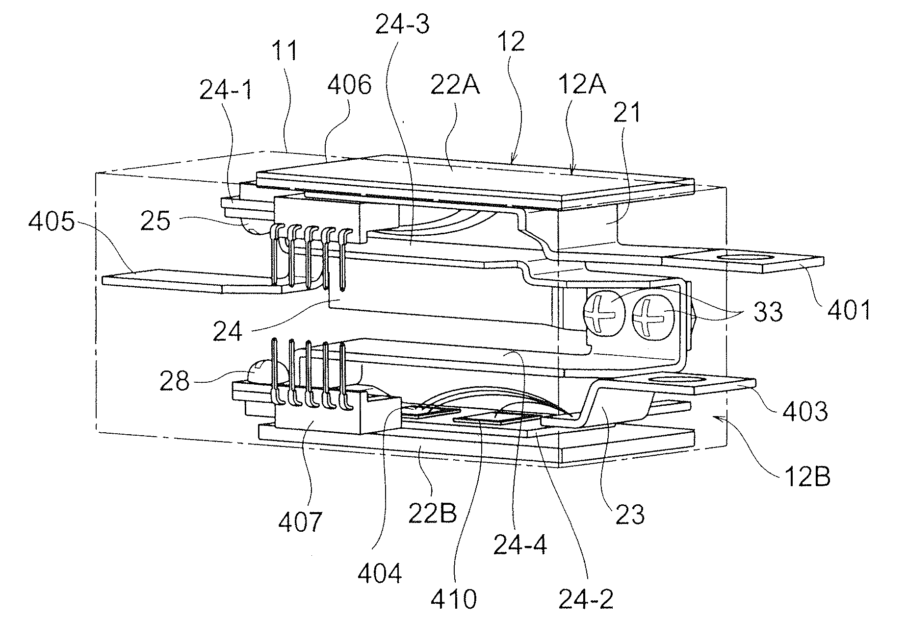
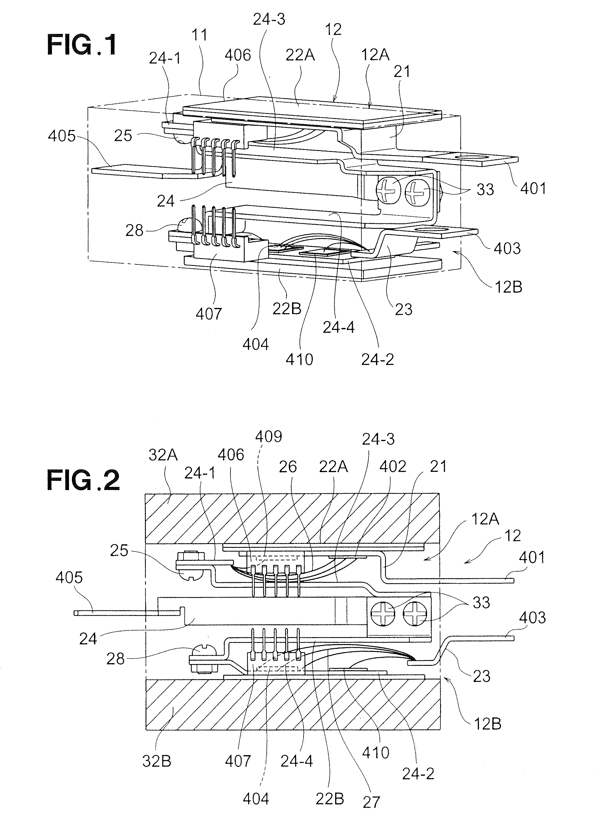
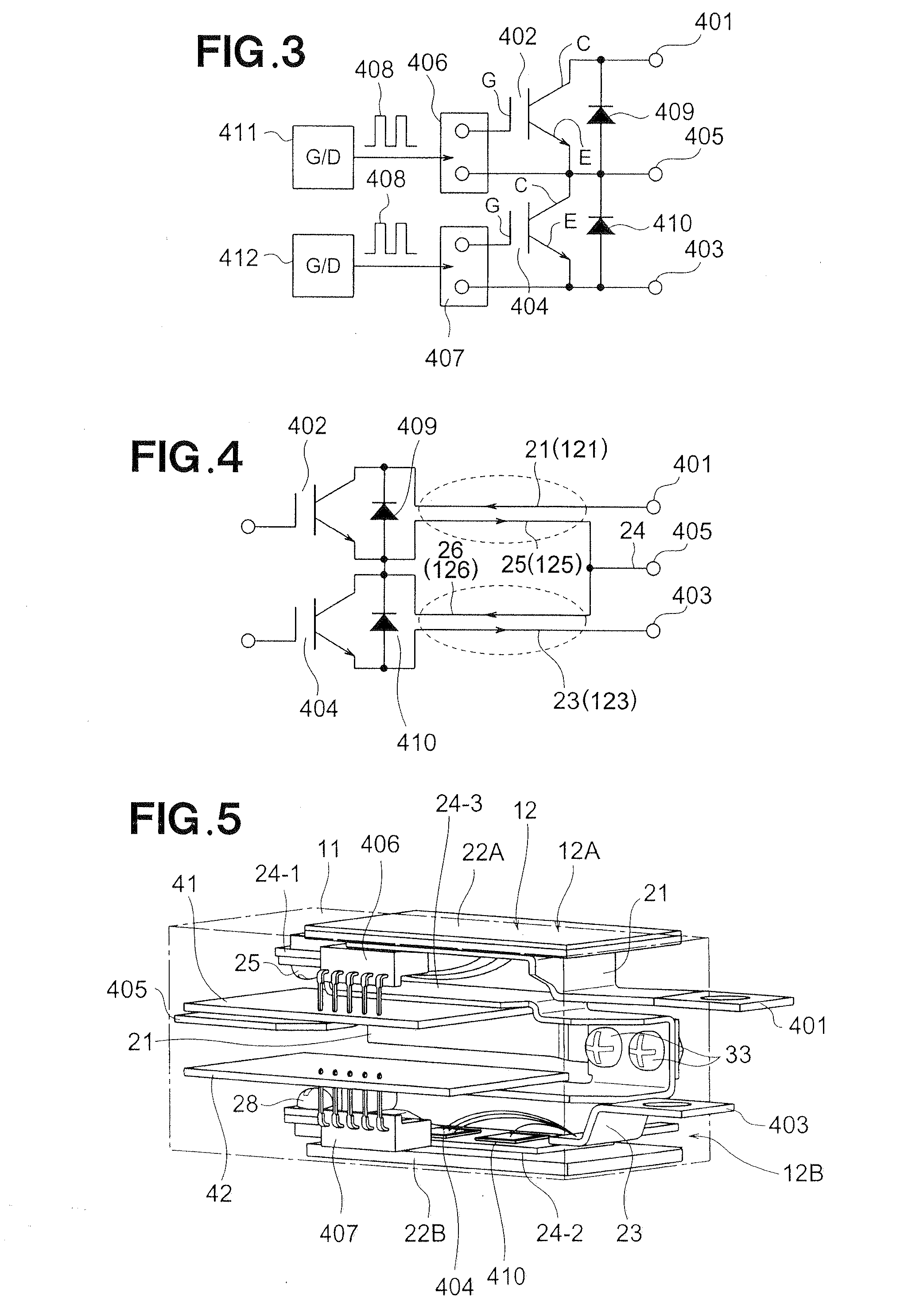
[0040]A semiconductor device according to the present invention will be described with reference to FIGS. 1 through 4. FIG. 1 shows the exterior of the semiconductor device and shows the modular structure of an IGBT module. FIG. 2 is a side view from the left side of FIG. 1. FIG. 3 is a circuit-configuration diagram of the electrical circuit of the IGBT module shown in FIG. 1, and FIG. 4 shows the characteristic relationships of the wirings of the IGBT module.

[0041]The semiconductor device according to the present embodiment is a power semiconductor device, and is typically an inverter device for driving a three-phase motor that drives an electric vehicle. The IGBT module shown in FIG. 1 displays the main portions of the inverter device. The configuration of the electrical circuit of the IGBT module will be described first with reference to FIG. 3.

[0042]FIG. 3 shows the electrical circuit portions of a single phase (one phase from among the U, V, or W phases) of the bridge circuit o...

second embodiment

[0086]According to the semiconductor device of the second embodiment, the aforedescribed control substrates 41, 42 that include the gate drivers 411; 412 are positioned using the space between the first assembly 12A and the second assembly 12B. The semiconductor device can therefore be made smaller and more compact.

[0087]In the output bus bar 24 that connects to the output terminal, the region from the bonding portion of the third metal wiring board 24-3 and the fourth metal wiring board 24-4 to the location corresponding to the position of the current sensors 43 is disposed in a perpendicular positional relationship relative to the surface that includes the control substrates 41, 42 on the lateral exterior side of the first and second control substrates 41, 42. According to this configuration, the portions of the output bus bar 24 other than those that correspond to the current sensors 43 formed as magnetic resistance elements are positioned outside the control substrates 41, 42; t...

third embodiment

[0091]According to the semiconductor device of the third embodiment, the high-voltage bus bar 21, the low-voltage bus bar 23, and the output bus bar 24A are provided on the same side in the IGBT module 12. The semiconductor device is made compact, and the output bus bar 24A is positioned in a location removed from the first and second control substrates 41, 42. The effect of output noise on the control substrates 41, 42 can therefore be limited.

[0092]In the description of these embodiments, an N-channel IGBT element was used as the power semiconductor element employed in the semiconductor device. In this instance, the power semiconductor elements in the semiconductor chips are IGBT elements (N-channel type). In the semiconductor chip of the first assembly 12A, a first surface is the collector-side surface, and the other surface is the emitter-side surface. In the semiconductor chip of the second assembly 12B, a first surface is the emitter-side surface, and the other surface is the ...


PUM


Abstract

A semiconductor device includes first and second assembled bodies (12A, 12B). The first assembled body is provided with a first semiconductor chip, a high voltage bus bar (21) connected to one surface of the first semiconductor chip, a first metal wiring board (24-1) connected to the other surface of the first semiconductor chip with a bonding wire, and a third metal wiring board (24-3) connected to the first metal wiring board. The second assembled body is provided with a second semiconductor chip, a low voltage bus bar (23) connected to one surface of the second semiconductor chip with a bonding wire, a second metal wiring board (24-2) connected to the other surface of the second semiconductor chip, and a fourth metal wiring board (24-4) connected by being returned from an end portion of the second metal wiring board and arranged in parallel to the second metal wiring board. The first assembled body and the second assembled body are arranged in a stacked structure wherein the assembled bodies are being separated. Inductance of a main circuit is reduced by the semiconductor module structure.

Description

TECHNICAL FIELD[0001]The present invention relates to a semiconductor device and, more particularly, to a semiconductor device that includes an IGBT module or the like used in a driving circuit for driving a driving motor of an electric vehicle.BACKGROUND ART[0002]Inverter devices are used to drive the driving motors of electric automobiles and other electric vehicles. These inverter devices include an electrical circuit in which switching elements are connected using a bridge-circuit configuration. Inverter devices turn the switching elements of the bridge circuit on and off as appropriate and execute the switching of current made to flow to the driving motor. Power transistors, IGBT, FET, and the like are widely used as the switching elements that constitute the bridge circuit. These inverter devices are usually configured in a modular structure in which a plurality of switching elements is housed in one package.[0003]The operation of the driving motor of an electric vehicle is ch...

Claims


Application Information

Patent Timeline
Patent Type & Authority Applications(United States)
IPC IPC(8): H05K1/14
CPCH01L25/071H01L25/18H01L2924/3011H01L2924/13091H01L2224/48091H01L2924/30107H01L2224/49113H01L2224/48247H01L2924/1305H01L2924/13055H01L2924/00014H01L2924/00
Inventor TAKANO, FUMITOMOWATANABE, SHINYAAIBA, TSUKASANAKASHIMA, JOJIOTSUKA, HIROSHI
Owner HONDA MOTOR CO LTD
Why Eureka
Try Eureka