Emission tuning methods and devices fabricated utilizing methods

a technology of emission tuning and emission characteristics, applied in semiconductor/solid-state device testing/measurement, manufacturing tools, instruments, etc., can solve the problems of difficult to consistently reproduce leds with the same or similar emission characteristics, difficult to control the geometry and thickness of phosphor layers, and non-uniform color temperature, etc., to achieve high yield of led chips, control the emission characteristics of led chips, and reduce the amount of conversion materials

Active Publication Date: 2009-10-22
CREELED INC
View PDF53 Cites 85 Cited by
  • Summary
  • Abstract
  • Description
  • Claims
  • Application Information

AI Technical Summary

Benefits of technology

[0019]The present invention discloses new methods for fabricating semiconductor devices such as LED chips at the wafer level, and discloses LED chips and LED chip wafers fabricated using the methods. The present invention is directed to controlling the emission characteristics of LED chips by altering the amount of LED light that is converted by the LED chip's conversion material. On way of altering the amount of light that is converted is by reducing the amount of conversion material over the LEDs. The methods according to the present invention are particularly applicable to altering the conversion material over LED chips at the wafer level to provide a high yield of LED chips emitting approximately at a target emission characteristic or within a range of emission characteristics, such as a chromaticity region on a CIE Curve. The present invention can also be utilized for fabricating LED chips at a wafer level with having a high yield of emissions within a stand deviation by MacAdam ellipses, such as a 4-step MacAdam ellipse.

Problems solved by technology

Using this method, however, the phosphor layer's geometry and thickness can be difficult to control.
As a result, light emitting from different coated LEDs can vary, and light emitted at different angles can pass through different amounts of conversion material, which can result in an LED with non-uniform color temperature as a function of viewing angle.
Because the geometry and thickness is hard to control, it can also be difficult to consistently reproduce LEDs with the same or similar emission characteristics.
Like the syringe method above, using the stencil method it can be difficult to control the geometry and layer thickness of the phosphor containing polymer.
The stenciling composition may not fully fill the stencil opening such that the resulting layer is not uniform.
These problems can result in LEDs having non-uniform color temperature and LEDs that are difficult to consistently reproduce with the same or similar emission characteristics.
Perceptible variations in color emitted by packages designed to emit a single color of light can reduce customer satisfaction and reduce overall acceptance of LED packages for commercial uses.
This binning process typically increases the manufacturing cost of LEDs by the overhead associated with the testing and separation of devices with different emission characteristics, and the formulation of the data and records surrounding this process.
The greater the number of bins for a particular LED being manufactured, the greater the additional cost associated with the binning process.
This in turn can result in increased end cost for the LEDs.

Method used


Image

  • Emission tuning methods and devices fabricated utilizing methods
  • Emission tuning methods and devices fabricated utilizing methods
  • Emission tuning methods and devices fabricated utilizing methods

Examples


Embodiment Construction

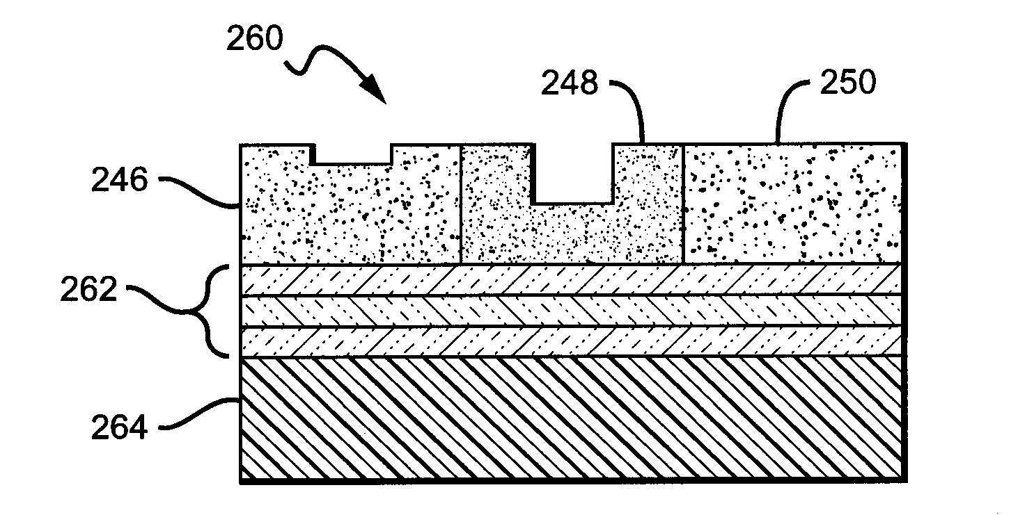
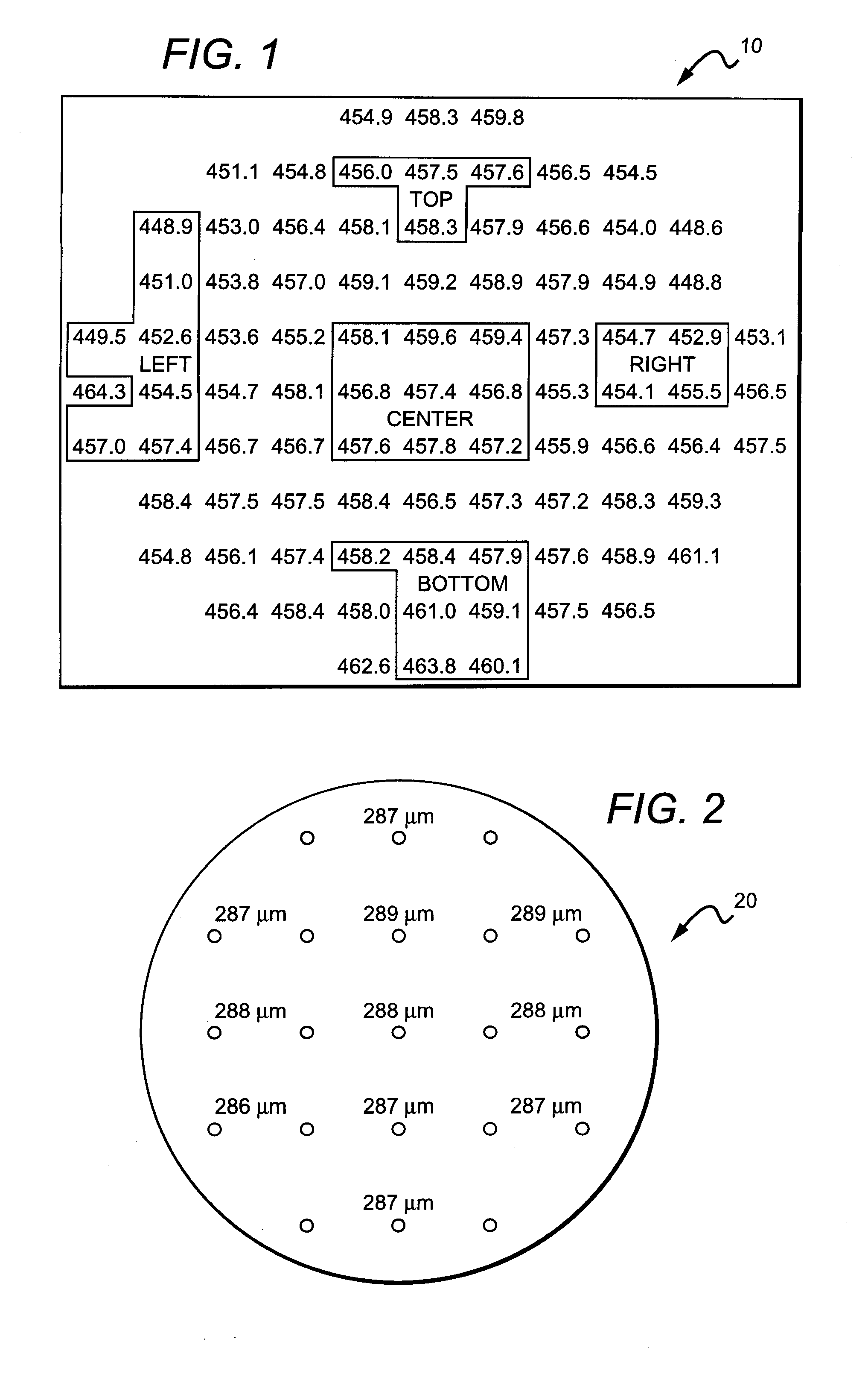
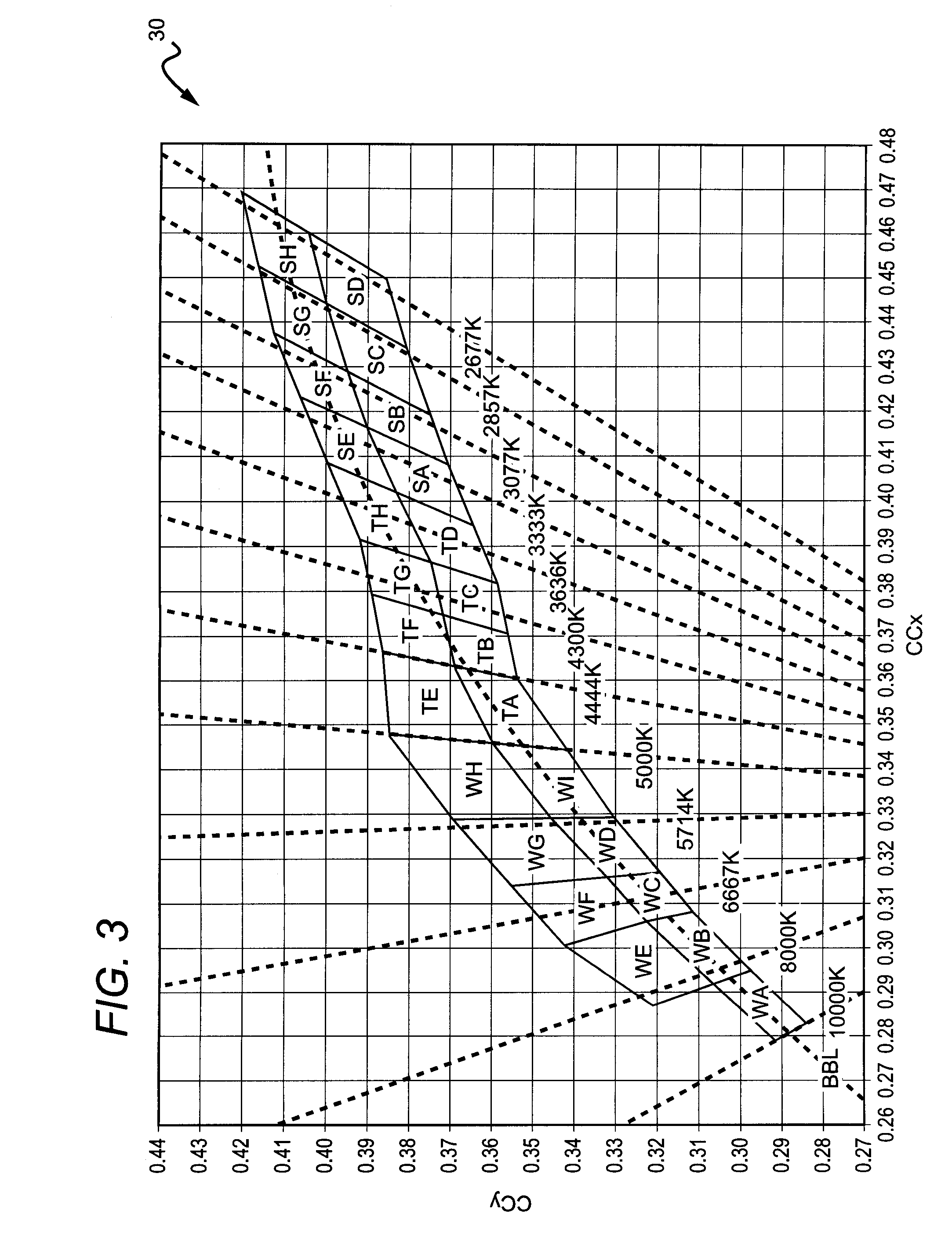
[0047]The present invention is directed to methods for tuning the emission characteristics of solid state emitters by altering the amount of conversion material over emitters, and is also directed to emitters fabricated using the methods. The present invention provides fabrication methods that are particularly applicable to wafer level fabrication of LEDs and altering the conversion material at the wafer level to reduce or eliminate the variations in emission characteristics of LED chips across the wafer. The methods according to the present invention can also be used to alter the emission characteristics of individual LEDs or groups of LEDs singulated from a wafer.

[0048]The present invention can be used to fabricate different LED chips but is particularly applicable to fabricating white emitting LED chips. In one such embodiment, a wafer of blue emitting LEDs having a dominant emission wavelength for example of between approximately 440 to 480 nm can be coated with a conversion mat...


PUM

PropertyMeasurementUnit
wavelength distributionaaaaaaaaaa
thicknessaaaaaaaaaa
emission wavelengthaaaaaaaaaa

Abstract

A method for fabricating light emitting diode (LED) chips comprising providing a plurality of LEDs, typically on a wafer, and coating the LEDs with a conversion material so that at least some light from the LEDs passes through the conversion material and is converted. The light emission from the LED chips comprises light from the conversion material, typically in combination with LED light. The emission characteristics of at least some of the LED chips is measured and at least some of the conversion material over the LEDs is removed to alter the emission characteristics of the LED chips. The invention is particularly applicable to fabricating LED chips on a wafer where the LED chips have light emission characteristics that are within a range of target emission characteristics. This target range can fall within an emission region on a CIE curve to reduce the need for binning of the LEDs from the wafer. The emission characteristics of the LED chips in the wafer can be tuned to the desired range by micro-machining the conversion material over the LEDs.

Description

[0001]This application claims the benefit of U.S. Provisional Patent Application Ser. No. 61 / 072,546 to Chitnes et al. al.BACKGROUND OF THE INVENTION[0002]1. Field of the Invention[0003]This invention relates to methods for fabricating sold state emitters and in particular methods for tuning the emission characteristics of light emitting diodes coated by a conversion material.[0004]2. Description of the Related Art[0005]Light emitting diodes (LED or LEDs) are solid state devices that convert electric energy to light, and generally comprise one or more active layers of semiconductor material sandwiched between oppositely doped layers. When a bias is applied across the doped layers, holes and electrons are injected into the active layer where they recombine to generate light. Light is emitted from the active layer and from all surfaces of the LED.[0006]Conventional LEDs cannot generate white light from their active layers. Light from a blue emitting LED has been converted to white lig...

Claims


Application Information

Patent Timeline
Patent Type & Authority Applications(United States)
IPC IPC(8): H01L33/00H01L21/66B23B47/00H01L33/50
CPCH01L33/0095H01L33/508Y10T408/47H01L2224/13H01L2933/0041
Inventor CHITNIS, ASHAYEDMOND, JOHNBRITT, JEFFREY CARLKELLER, BERND P.EMERSON, DAVID TODDBERGMANN, MICHAEL JOHNCABALU, JASPER S.
Owner CREELED INC
Why Eureka
Try Eureka