Semiconductor devices for high power application

a high-power application and semiconductor technology, applied in the field of semiconductor devices, can solve the problems of limiting the voltage tolerance of transistors, consuming a lot of space, and difficult device integration, so as to reduce the distance between the devices, maintain the voltage tolerance, and increase the manufacturing yield

Active Publication Date: 2009-10-22
VANGUARD INTERNATIONAL SEMICONDUCTOR CORPORATION
View PDF4 Cites 12 Cited by
  • Summary
  • Abstract
  • Description
  • Claims
  • Application Information

AI Technical Summary

Benefits of technology

[0012]In order to overcome the disadvantageous mentioned above, the invention provides a high voltage (high power) semiconductor device wh

Problems solved by technology

However, the device region isolated by the P-type deep heavily doped regions 19 occupies too much area, which makes device integration difficult.
However, LDMOSFET's raise voltage tolerances by inc

Method used


Image

  • Semiconductor devices for high power application
  • Semiconductor devices for high power application
  • Semiconductor devices for high power application

Examples


Embodiment Construction

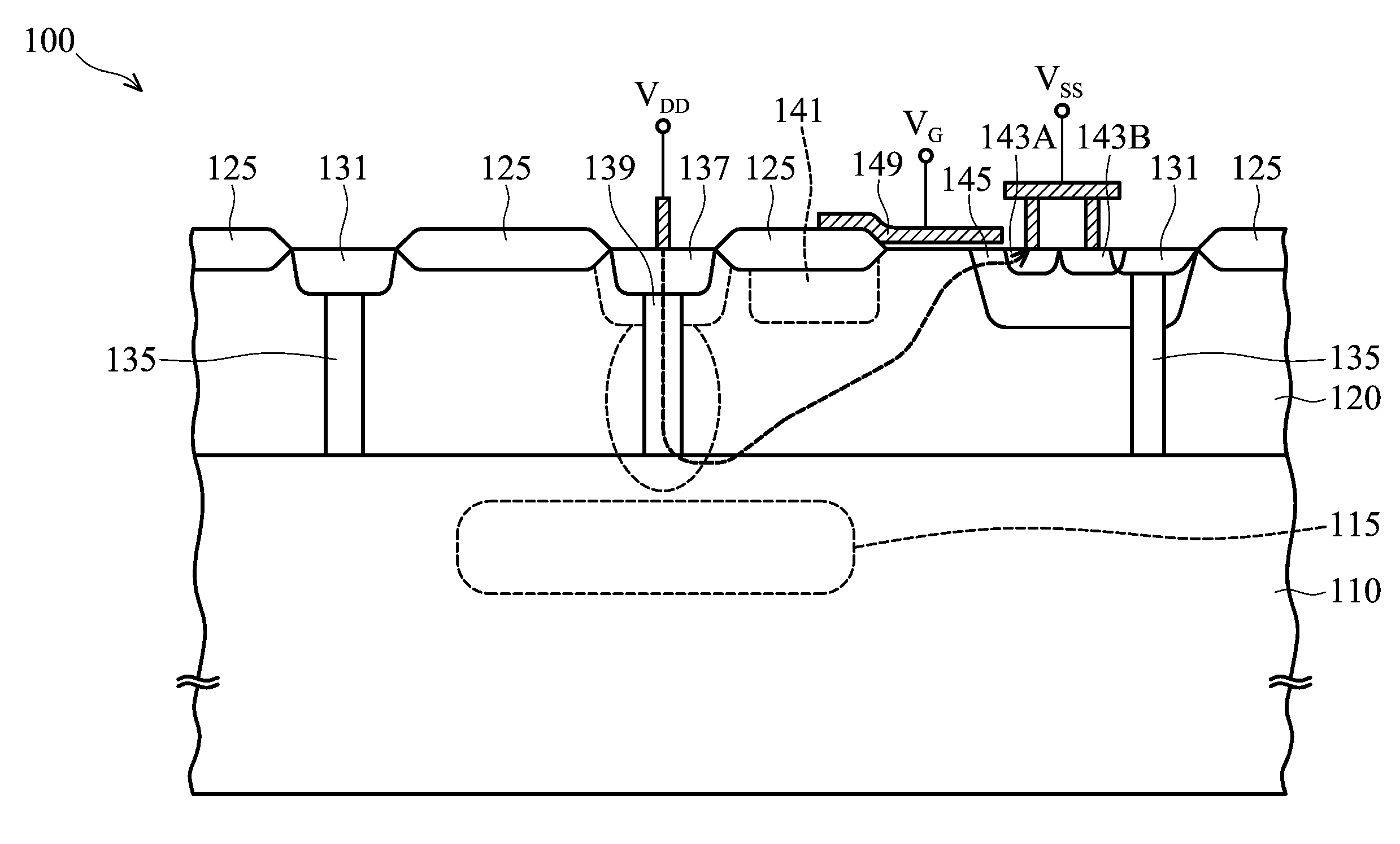
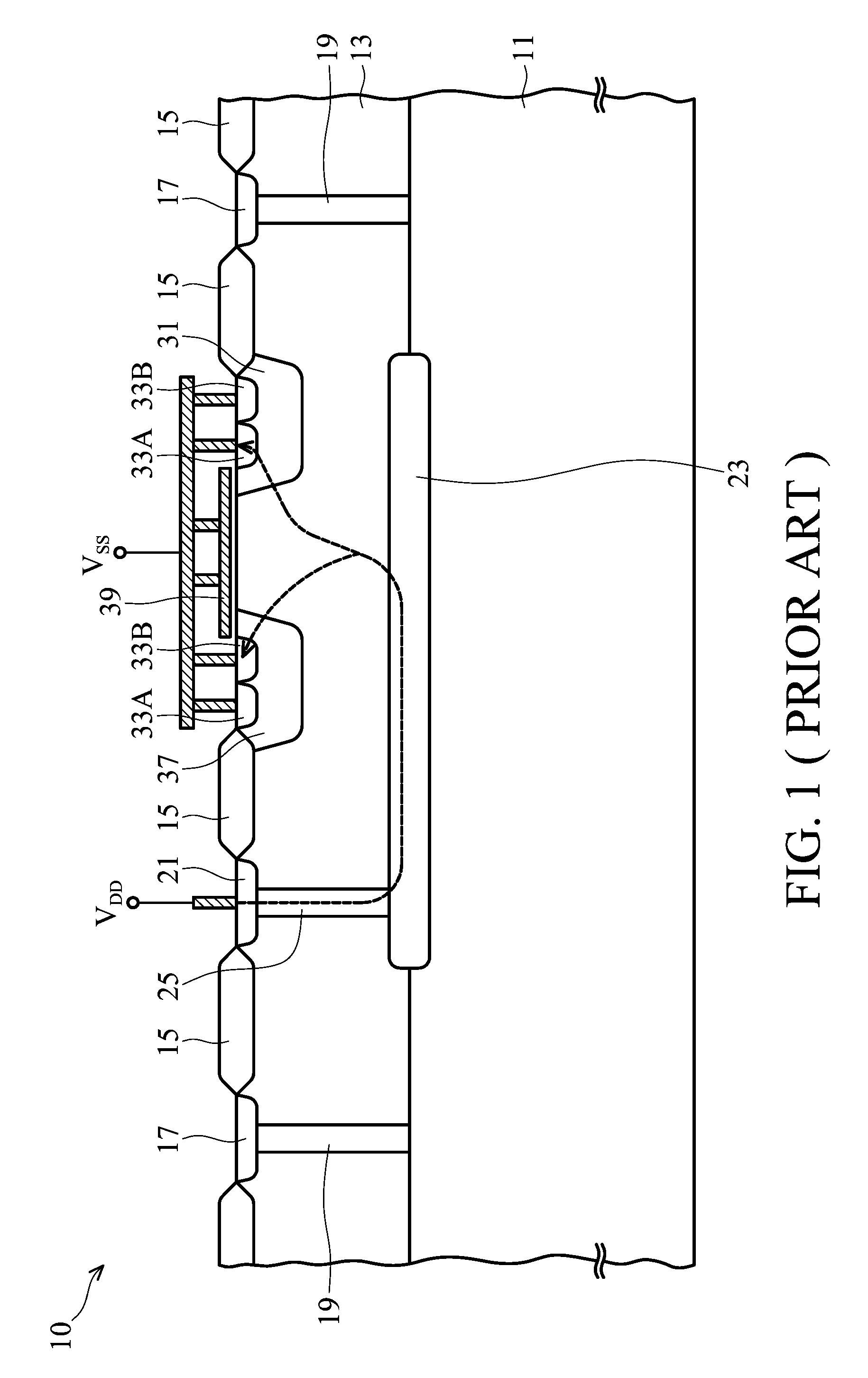
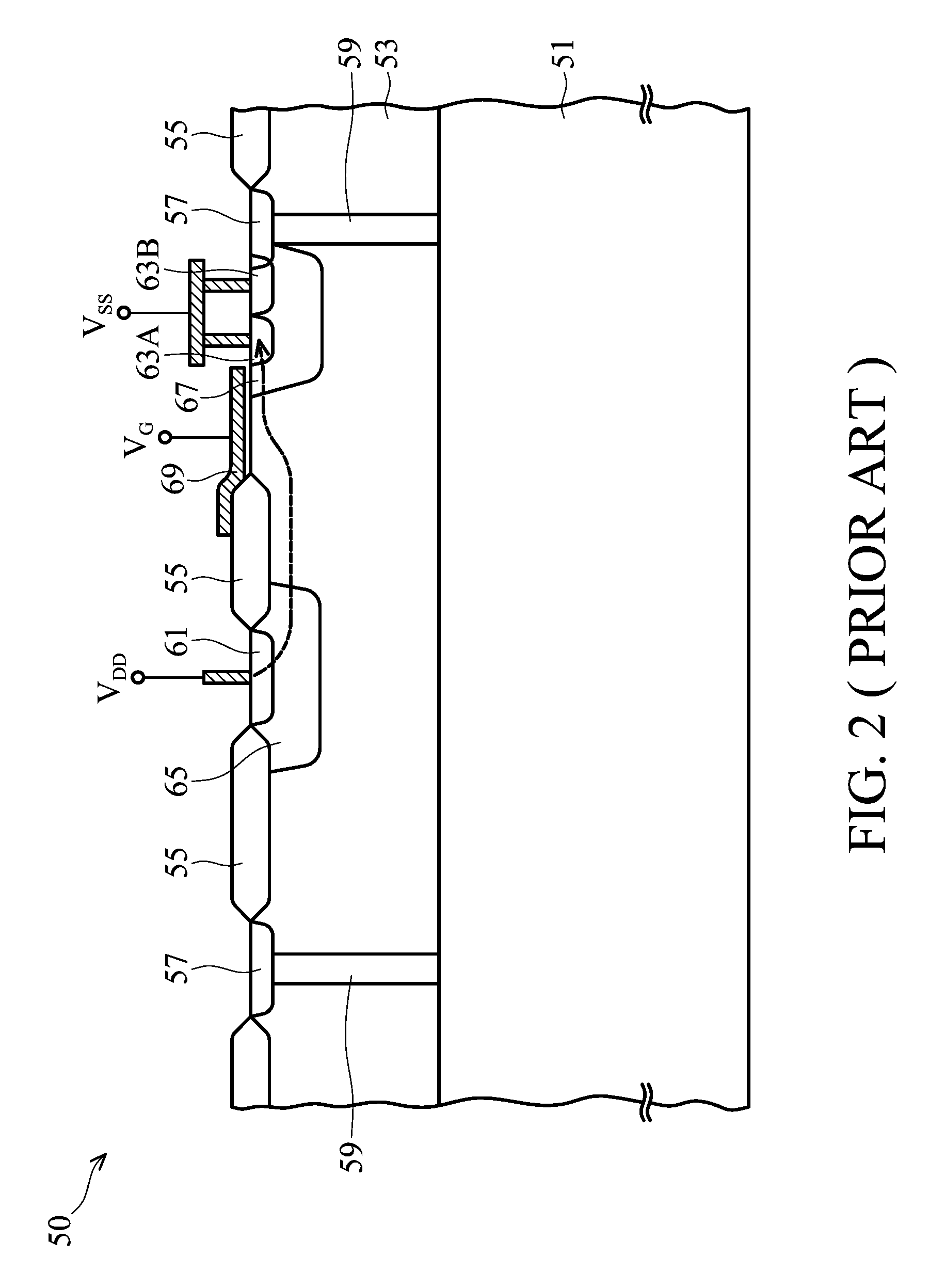
[0023]The following description is of the best-contemplated mode of carrying out the invention. This description is made for the purpose of illustrating the general principles of the invention and should not be taken in a limiting sense. The scope of the invention is best determined by reference to the appended claims.

[0024]Reference will be made in detail to the present embodiments, examples of which are illustrated in the accompanying drawings. Wherever possible, the same reference numbers are used in the drawings and the description to refer to the same or like parts. In the drawings, the shape and thickness of one embodiment may be exaggerated for clarity and convenience. This description will be directed in particular to elements forming part of, or cooperating more directly with, apparatus in accordance with the present invention. It is to be understood that elements not specifically shown or described may take various forms well known to those skilled in the art. Further, the...


PUM


Abstract

Semiconductor devices for high voltage application are presented. A high power semiconductor device includes a first type doped semiconductor substrate and a second type doped epitaxial layer deposited thereon. A first type doped body region is disposed in the second type doped epitaxial layer. A heavily doped drain region is formed in the second type doped epitaxial layer and isolated from the first type doped body region with an isolation region and a channel. A second type deep heavily doped region extends from the heavily doped drain region to the semiconductor substrate. A pair of inversed type heavily doped source regions is disposed in the first type doped body region. A gate electrode is disposed overlying the channel with a dielectric layer interposed therebetween. The high power semiconductor device is isolated from the other semiconductor devices with a first type deep heavily doped region.

Description

CROSS REFERENCE TO RELATED APPLICATIONS[0001]This Application claims priority of Taiwan Patent Application No. 097114479, filed on Apr. 21, 2008, the entirety of which is incorporated by reference herein.BACKGROUND OF THE INVENTION[0002]1. Field of the Invention[0003]The present invention relates to a semiconductor device, and in particular relates to a PIN diode device and the method for forming thereof.[0004]2. Description of the Related Art[0005]High power semiconductor devices are applied to integrated circuits with high voltage and high power. Traditional high power semiconductor devices are mainly used for devices with at least 18 volts or higher. The advantages of high power device technology include cost effectiveness and process compatibility. High power device technology has been widely used in display driver IC devices, power supply devices, power management fields, communications fields, autotronics fields, and industrial control fields, etc.[0006]Traditional high power ...

Claims


Application Information

Patent Timeline
IPC IPC(8): H01L29/78
CPCH01L29/0634H01L29/0696H01L29/0878H01L29/7816H01L29/1095H01L29/42368H01L29/7809H01L29/1083
Inventor TSAI, HUNG-SHERNLIN, GEENG-LIHLIANG, WEN-JYA
Owner VANGUARD INTERNATIONAL SEMICONDUCTOR CORPORATION
Why Eureka
Try Eureka