Integrated inductor

a technology of integrated inductors and semiconductor substrates, applied in the direction of semiconductor devices, semiconductor/solid-state device details, inductance, etc., can solve the problems of reduced resistance of integrated inductors fabricated by rf baseline process, limited quality factor q of integrated circuits, etc., to reduce parasitic substrate coupling, increase the distance between the bottom surface of the inductor structure and the main surface of the semiconductor substrate, and increase the thickness of the passivation layer

Active Publication Date: 2009-10-22
MEDIATEK INC
View PDF37 Cites 13 Cited by
  • Summary
  • Abstract
  • Description
  • Claims
  • Application Information

AI Technical Summary

Benefits of technology

[0009]It is one object of the invention to provide a monolithic integrated inductor with simple process, low cost and high Q factor.
[0011]In one aspect of this invention, according to another embodiment, an integrated inductor includes a winding consisting of an aluminum layer atop a passivation layer, wherein the aluminum layer does not extend into the passivation layer and has a thickness that is not less than about 2.0 micrometers. The passivation layer has a thickness not less than about 0.8 micrometers. By eliminating copper from the integrated inductor structure and increasing the thickness of the passivation layer, the distance between the bottom surface of the inductor structure and the main surface of the semiconductor substrate is increased, thus the parasitic substrate coupling may be reduced and the Q-factor may be improved. Besides, the increased thickness of the aluminum layer may help improve the Q-factor as well.
[0012]According to the embodiment, the distance D between the bottom surface of the inductor structure and the main surface of the semiconductor substrate may be greater than 3.0 micrometers for high Q-factor performance in an advanced integrated circuit chip.

Problems solved by technology

The quality factor Q of an integrated circuit is limited by parasitic losses within the substrate itself.
These losses include high resistance through metal layers of the inductor itself.
Therefore, integrated inductors fabricated by RF baseline process may have decreased resistance due to much thicker top metal layer (i.e., the topmost level of the damascene copper interconnection).
However, such ultra thick metal layer leads to complicated process and relatively lower throughput and higher cost.

Method used


Image

  • Integrated inductor
  • Integrated inductor
  • Integrated inductor

Examples


Embodiment Construction

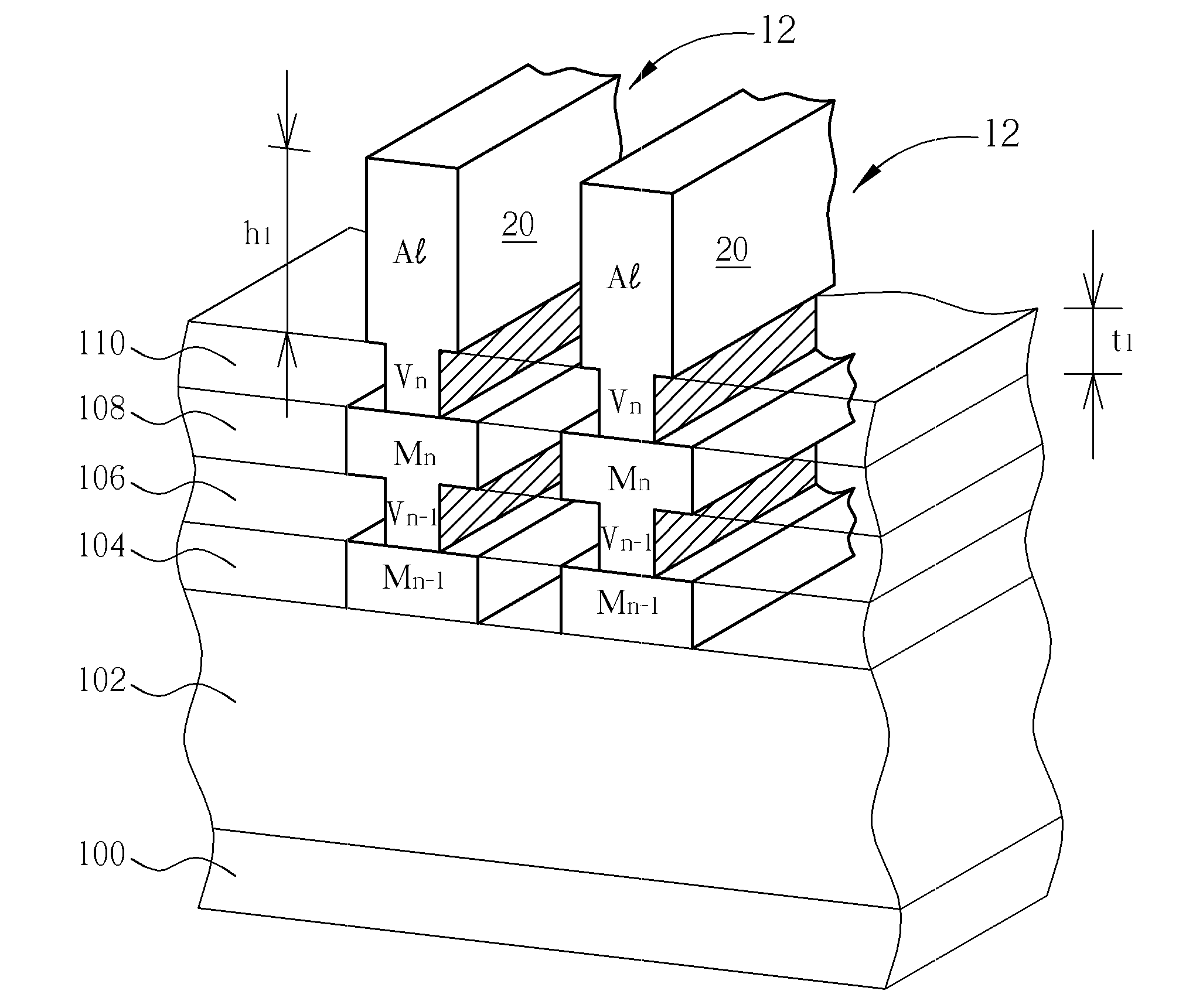
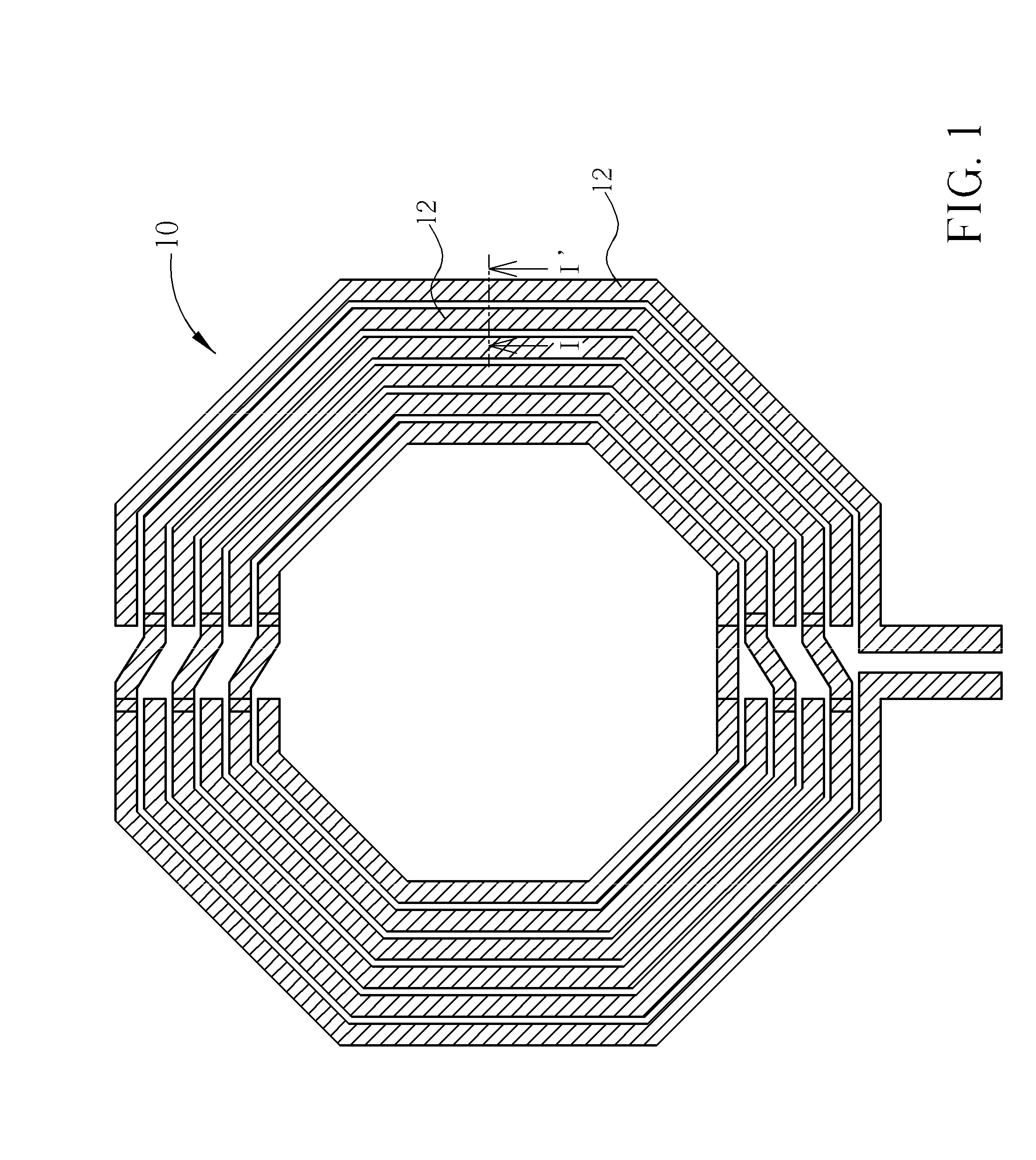
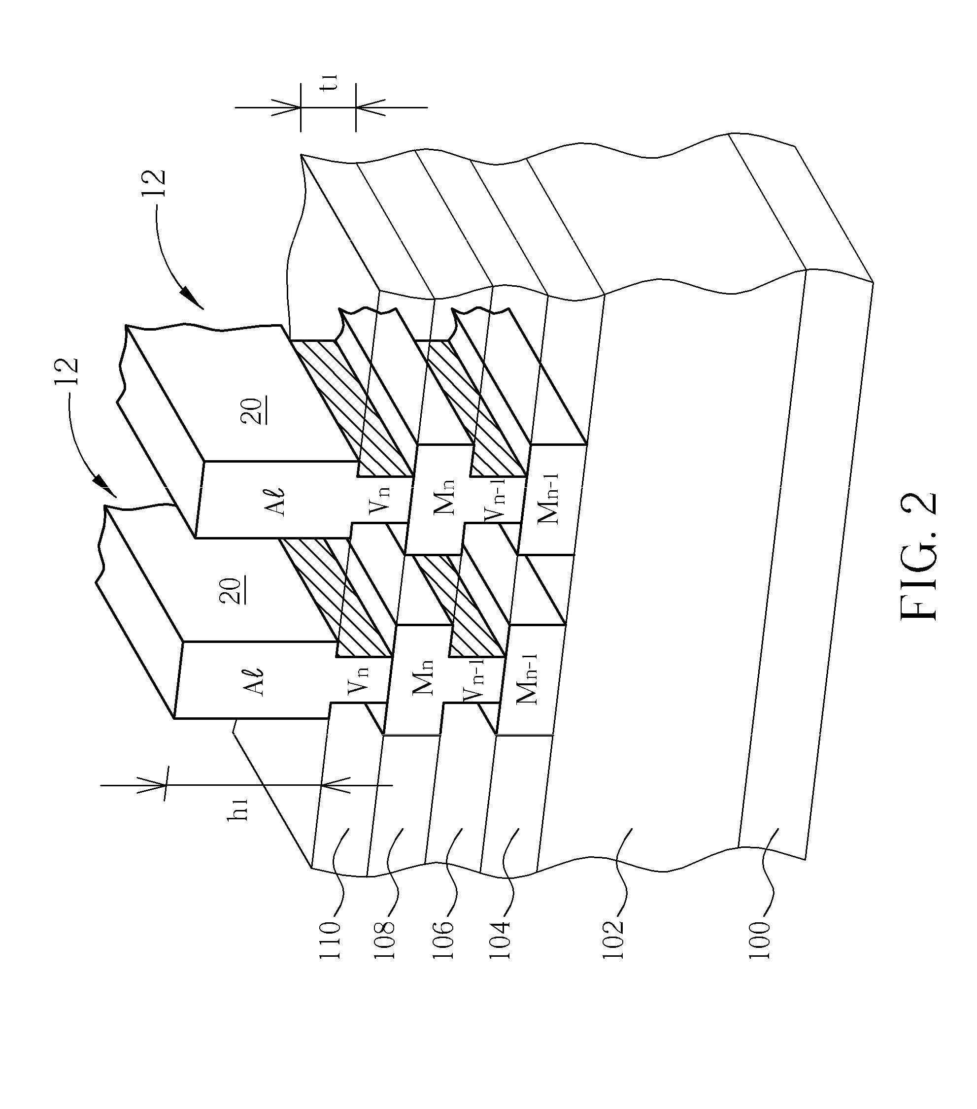
[0018]The invention pertains to an improved integrated inductor or transformer structure capable of improving the quality factor Q and reducing undesired substrate coupling. The manufacture cost can also be reduced. From one aspect, the invention uses line-shaped via structure, instead of hole-shaped via plug, for electrically connecting an upper level metal with a lower level metal. Conventionally, there are many via plugs deposed between conductive layers in a semiconductor device for electrically connection the conductive layers. In order to keep process uniformity, the conventional hole-shaped via plugs have a uniform shape and size. Therefore, for the sake of reduce resistance, an array of via plugs is utilized.

[0019]From another aspect of the invention, a layer of metal, such as aluminum, over the passivation layer of the integrated circuit chip is employed to fabricate the integrated inductor such that the topmost copper metal layer of the integrated circuit chip has a reduce...


PUM

PropertyMeasurementUnit
thicknessaaaaaaaaaa
thicknessaaaaaaaaaa
distanceaaaaaaaaaa

Abstract

An integrated inductor includes a winding consisting of an aluminum layer atop a passivation layer, wherein the aluminum layer does not extend into the passivation layer and has a thickness that is not less than about 2.0 micrometers. The passivation layer has a thickness not less than about 0.8 micrometers. By eliminating copper from the integrated inductor and increasing the thickness of the passivation layer, the distance between the bottom surface of the inductor structure and the main surface of the semiconductor substrate is increased, thus the parasitic substrate coupling may be reduced and the Q-factor may be improved. Besides, the increased thickness of the aluminum layer may help improve the Q-factor as well.

Description

CROSS REFERENCE TO RELATED APPLICATIONS[0001]This application is a continuation-in-part of U.S. application Ser. No. 11 / 768,199 filed Jun. 26, 2007. This application also claims the benefit of U.S. provisional application No. 61 / 180,164 filed May 21, 2009.BACKGROUND OF THE INVENTION[0002]1. Field of the Invention[0003]The invention relates generally to the field of semiconductor integrated circuit design, and more particularly, to an on-chip high-Q (high quality factor) integrated inductor structure.[0004]2. Description of the Prior Art[0005]The fast growing of the wireless market has created an urgent demand for smaller and cheaper handsets with increased functionality and performance. A major trend of circuit design is to incorporate as many circuit components into integrated circuit form as possible, whereby cost per wafer can be reduced.[0006]Inductors built in semiconductor wafers are widely used in CMOS based radio frequency (RF) circuits such as low-noise amplifiers, voltage-...

Claims


Application Information

Patent Timeline
Patent Type & Authority Applications(United States)
IPC IPC(8): H01F5/00
CPCH01L23/5227H01L28/10H01L2924/0002H01L2924/00
Inventor KO, CHING-CHUNGLEE, TUNG-HSINGCHAN, KUEI-TICHENG, TAOYANG, MING-TZONG
Owner MEDIATEK INC
Why Eureka
Try Eureka