Reflective Positive Electrode And Gallium Nitride-Based Compound Semiconductor Light-Emitting Device Using The Same

a technology of positive electrode and compound semiconductor, which is applied in the direction of semiconductor devices, basic electric elements, electrical equipment, etc., can solve the problems of low contact, low contact, and inability to provide the electrode on the rear surface of the substrate, so as to achieve good electrical characteristics, reduce contact resistance, and reduce the effect of reverse voltag

Inactive Publication Date: 2009-10-22
RESONAC HOLDINGS CORPORATION
View PDF9 Cites 12 Cited by
  • Summary
  • Abstract
  • Description
  • Claims
  • Application Information

AI Technical Summary

Benefits of technology

[0009]It is an object of the present invention to provide a gallium nitride-based compound semiconductor light-emitting device which resolves the above-described problem associated with Ag and Al, namely, which has a highly reflective positive electrode that has high reverse voltage and excellent reliability with low contact resistance to the p-type gallium nitride-based compound semiconductor layer.
[0032]A reflective positive electrode for a semiconductor light-emitting device according to the present invention has a positive electrode contact metal layer of a platinum group metal inter posed between a p-type semiconductor layer and a positive electrode reflective layer of Ag or Al, so that diffusion of metal constituting the reflective layer, Ag or Al, into the p-type semiconductor layer is restrained, and therefore, the light-emitting device has good electrical characteristics and high reliability.
[0033]Contact resistance can be further reduced by providing a semiconductor-metal-containing layer containing a group III metal constituting the semiconductor on the surface of the positive electrode contact metal layer on the side of the semiconductor.
[0034]A gallium nitride base compound semiconductor light-emitting device according to the present invention has the contact resistance between the positive electrode and the p-type semiconductor further reduced by providing a positive-electrode-metal-containing layer containing the metal constituting the contact metal layer on the surface of the p-type semiconductor layer on the side of the positive electrode.
[0035]By forming the contact metal layer of the positive electrode by sputtering method using RF discharge, the positive-electrode-metal-containing layer and the semiconductor-metal-containing layer can be formed without an annealing process, so that productivity can be improved.
[0036]Also, by providing an overcoat layer so as to cover the side and upper surfaces of the reflective layer, the stability of the light-emitting device can be further improved.

Problems solved by technology

As this is an insulating substrate, unlike GaAs-based light-emitting devices, an electrode cannot be provided on rear surface of the substrate.
Therefore, low contact resistance and high reflectance are the properties required for the materials of positive electrode.
However, when Ag and Al diffuse excessively into the p-type semiconductor layer, small current leaks occur, leading to lowering of the reverse voltage.
This results, in a long-term aging test, in variation in characteristic values, and leads to a reduction in reliability.

Method used


Image

  • Reflective Positive Electrode And Gallium Nitride-Based Compound Semiconductor Light-Emitting Device Using The Same
  • Reflective Positive Electrode And Gallium Nitride-Based Compound Semiconductor Light-Emitting Device Using The Same

Examples


example 1

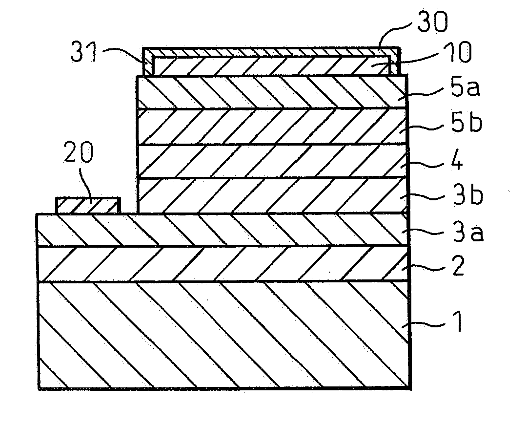
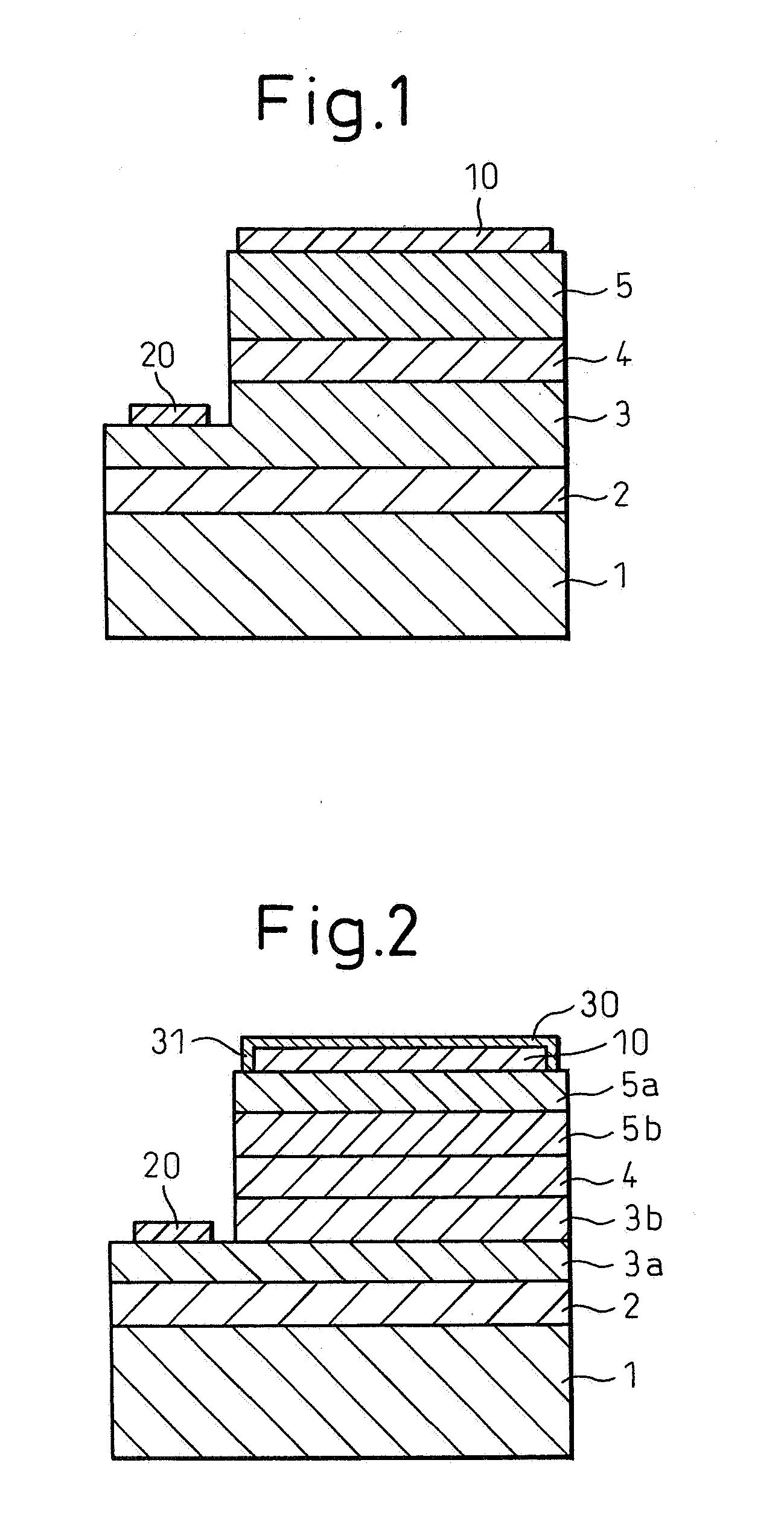
[0075]FIG. 2 is a schematic view showing a gallium nitride-based compound semiconductor light-emitting device fabricated in the present Example.

[0076]The gallium nitride-based compound semiconductor was formed by laminating a buffer layer 2 of ALN layer on a sapphire substrate 1, and by successively laminating thereon a n-contact layer 3a of n-type GaN layer, a n-clad layer 3b of n-type GaN layer, a light-emitting layer 4 of InGaN layer, a p-clad layer 5b of p-type AlGaN layer, a p-contact layer 5a of p-type GaN layer. The n-contact layer 3a is n-type GaN layer doped with Si at 7×10¹⁸ / cm3, and n-clad layer 3b is n-type GaN layer doped with Si at 5×10¹⁸ / cm3. The light-emitting layer 4 has single quantum well structure, and the composition of InGaN is In0.95Ga0.05N. The p-clad layer 5b is p-type AlGaN doped with Mg at 1×10¹⁸ / cm3, and the composition is Al0.25Ga0.75N. The p-contact layer 5a is p-type GaN layer doped with Mg at 5×10¹⁹ / cm3. Lamination of these layers were carried out...

examples [UNK]

Examples 9˜11

[0095]A gallium nitride-based compound semiconductor light-emitting device was fabricated in the same manner as in Example 1, except that heat treatment was conducted after forming Ag reflective layer, and characteristics of the device was evaluated as in Example 1. Heat treatment was conducted in a RTA furnace in air by varying the temperature for 10 minutes. Table 2 shows temperature of heat treatment and forward voltage. Forward voltage was somewhat higher in the light-emitting device subjected to heat treatment at 400° C.

TABLE 2Heating temperatureForward voltage(° C.)(V)Example 1—3.3Example 92003.3Example 103003.3Example 114003.8


PUM

PropertyMeasurementUnit
temperatureaaaaaaaaaa
thicknessaaaaaaaaaa
thicknessaaaaaaaaaa

Abstract

A gallium nitride-based compound semiconductor light-emitting device which has a highly reflective positive electrode that has high reverse voltage and excellent reliability with low contact resistance to the p-type gallium nitride-based compound semiconductor layer. The reflective positive electrode for a semiconductor light-emitting device comprises a contact metal layer adjoining a p-type semiconductor layer, and a reflective layer on the contact metal layer, wherein the contact metal layer is formed of a platinum group metal or an alloy containing a platinum group metal, and the reflective layer is formed of at least one metal selected from the group consisting of Ag, Al, and alloys containing at least one of Ag and Al. Also disclosed is a production method of the reflective positive electrode.

Description

CROSS REFERENCE TO RELATED APPLICATION[0001]This is a Continuation of application Ser. No. 11 / 629,306 which is a National Stage Application filed under §371 of PCT Application No. PCT / JP2005 / 011870 filed Jun. 22, 2005, and which claims benefit of JPA No. 2004-186871 filed Jun. 24, 2004 and U.S. Provisional Application No. 60 / 584,175 filed Jul. 1, 2004. The above-noted applications are incorporated herein by reference in their entirety.TECHNICAL FIELD[0002]The present invention relates to a reflective positive electrode for a light-emitting device and, more particularly, to a reflective positive electrode having excellent characteristics and stability, and to a flip chip type gallium nitride-based compound semiconductor light-emitting device using the same.BACKGROUND ART[0003]In recent years, a gallium nitride-based compound semiconductor represented by the formula AlxInyGa1-x-yN (0≦x<1, 0≦y<1, x+y<1) has attracted much attention as a material for a light-emitting diode (LED...

Claims


Application Information

Patent Timeline
Patent Type & Authority Applications(United States)
IPC IPC(8): H01L21/00H01L33/32H01L33/40
CPCH01L21/28575H01L33/405H01L33/32
Inventor KAMEI, KOJI
Owner RESONAC HOLDINGS CORPORATION
Why Eureka
Try Eureka