

Infrared detector and solid state image sensor having the same
a technology of infrared detector and solid-state image sensor, which is applied in the direction of optical radiation measurement, radiation control devices, instruments, etc., can solve the problems of increased manufacturing cost and insufficient sensitivity, and achieve the effect of low cost and efficient absorption of infrared rays
- Summary
- Abstract
- Description
- Claims
- Application Information
AI Technical Summary
Benefits of technology
Problems solved by technology
Method used
Image

Examples
first embodiment
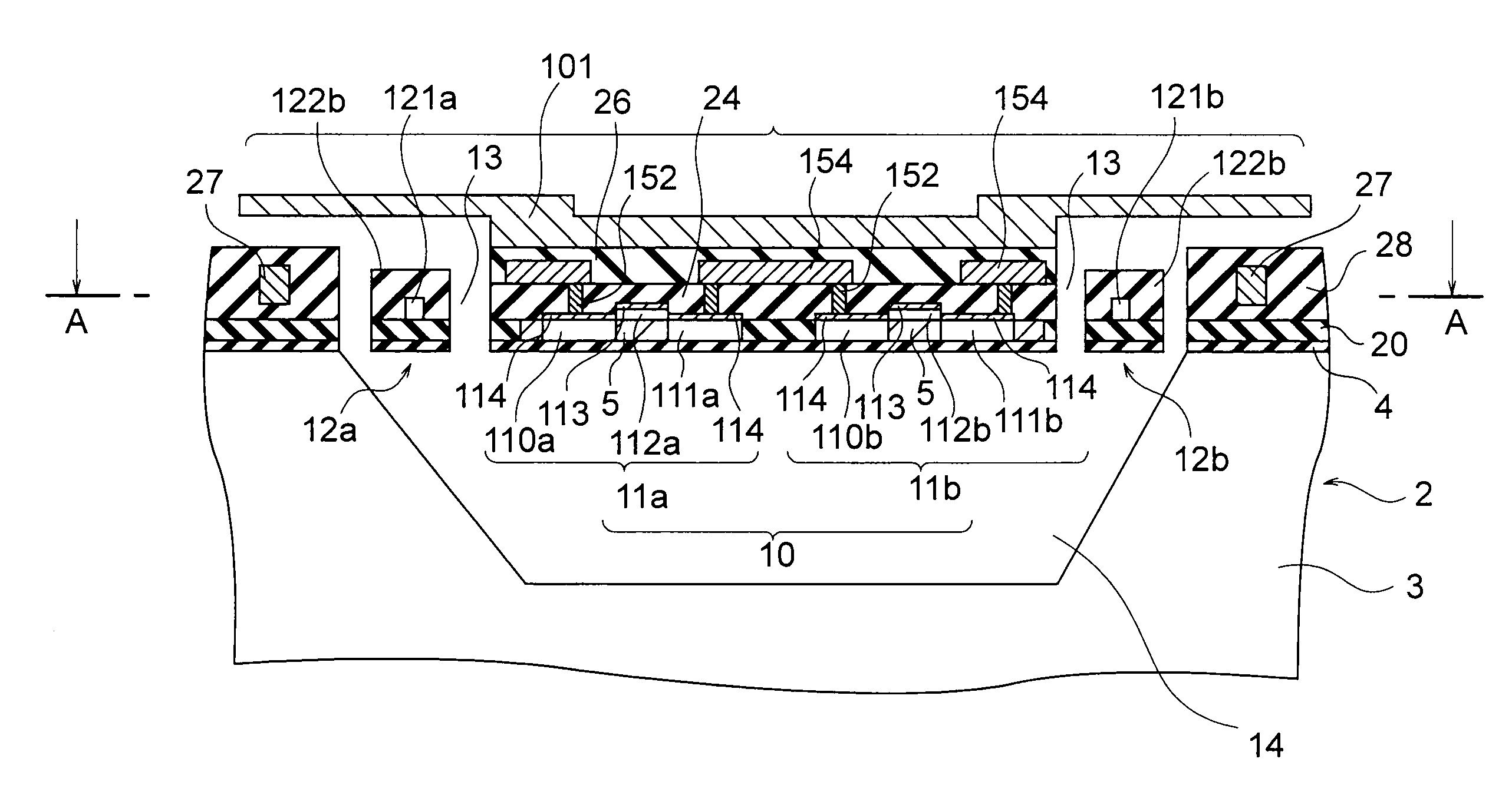
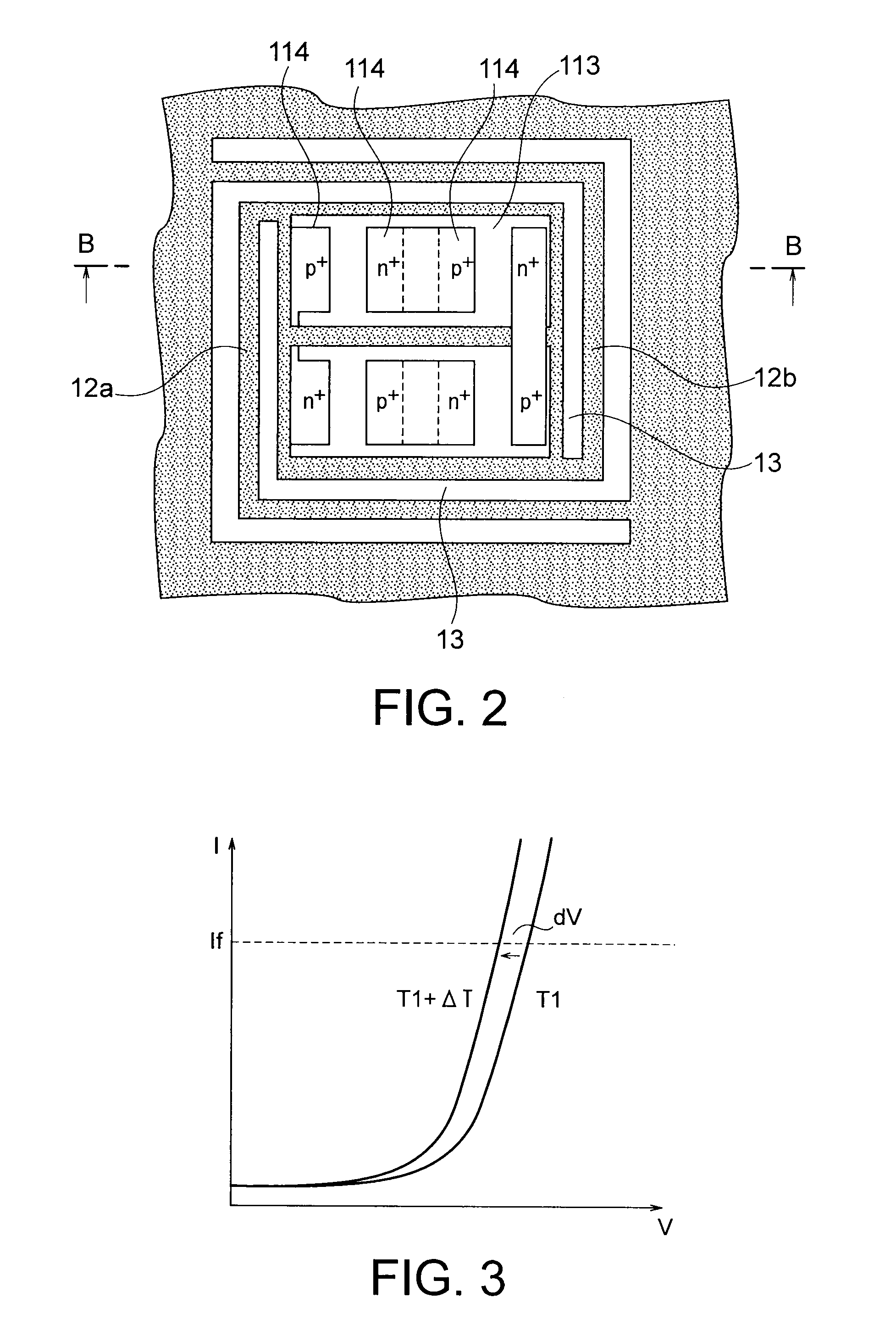
[0020]An infrared detector according to a first embodiment of the present invention is shown in FIGS. 1 and 2. FIG. 1 is a sectional view of the infrared detector according to the present embodiment. FIG. 2 is a plan view obtained by viewing a lower part from a cutting plane A-A shown in FIG. 1. FIG. 1 is a sectional view obtained by cutting along a cutting line B-B shown in FIG. 2.
[0021]An infrared detector 1 according to the present embodiment is formed in a SOI substrate 2 including a support substrate 3, a buried oxide film 4 and a SOI layer 5 formed of low concentration p-type silicon (hereafter referred to as p− type silicon). A plurality of thermoelectric conversion elements 11a and 11b, which will be described later, are formed in the SOI layer 5. The SOI layer except for the thermoelectric conversion elements 11a and 11b is replaced by an element isolation region 20 formed of, for example, silicon dioxide. A cavity portion (concave portion) 14 is provided on the buried oxid...
second embodiment
[0046]An infrared detector according to a second embodiment of the present invention is shown in FIG. 12. The infrared detector 1 according to the present embodiment is obtained from the infrared detector according to the first embodiment shown in FIG. 1 by forming the SOI layer 5 instead of the element isolation region 20 between the thermoelectric conversion elements 11a and 11b and forming a silicide layer 114a on surfaces of the SOI layer 5, the n-type silicon layer 111a and the p-type silicon layer 110b. Thus, the infrared detector 1 according to the present embodiment has a configuration in which the thermoelectric conversion elements 11a and 11b are connected in series. Therefore, the wiring 154 and the contacts 152 become unnecessary. As a result, the thermal capacity of the cell portion 10 can be reduced remarkably, and the thermal time constant τ can be made small. Accordingly, the thermal response of the cell portion 10 can be quickened.
third embodiment
[0047]An infrared detector according to a third embodiment of the present invention will now be described with reference to FIG. 13. FIG. 13 is a top view of the thermoelectric conversion elements 11a and 11b in the infrared detector according to the present embodiment.
[0048]The infrared detector according to the present embodiment is obtained from the infrared detector according to the first or second embodiment by forming the polysilicon layers 112a and 112b, respectively formed on regions between the p-type silicon layers 110a and 110b and the n-type silicon layers 111a and 111b respectively in the thermoelectric conversion elements 11a and 11b, in a winding form and providing the p-type silicon layers 110a and 110b and the n-type silicon layers 111a and 111b, which are isolated respectively by the polysilicon layers 112a and 112b, with comb teeth shapes.
[0049]As compared with the layout of the infrared detector according to the first or second embodiment, the area of the pn junc...
PUM
 Abstract
Description
Claims
Application Information