CuSiN/SiN DIFFUSION BARRIER FOR COPPER IN INTEGRATED-CIRCUIT DEVICES

a technology of integrated circuits and diffusion barriers, which is applied in semiconductor devices, semiconductor/solid-state device details, electrical apparatuses, etc., can solve the problems of poor adhesion between the known p-ulk/metal barrier/copper-containing material layer sequences, device performance issues, and decrease of reliability, so as to achieve high cmp-selectivity and reduce surface roughness

Active Publication Date: 2009-11-05
NXP BV
View PDF21 Cites 23 Cited by
  • Summary
  • Abstract
  • Description
  • Claims
  • Application Information

AI Technical Summary

Benefits of technology

[0037]In a further preferred embodiment, fabricating the feature comprises a step of planarizing a top surface of the dielectric layer by removing Copper and the CuSiN layer using a chemical mechanical polishing (CMP) process that is selective to Copper-containing material and does not remove underlying dielectrics. CMP processes, which provide selectivity to Copper-containing material and do not remove underlying dielectrics are per se known in the art. However, in the context of the present invention, due to the layer structure deposited on the surface, the high CMP-selectivity between the metal and the dielectric allows decreasing the surface roughness all over a wafer used for the fabrication of the integrated-circuit device.

Problems solved by technology

However, this strategy has several disadvantages.
The precursor used for the metallic diffusion-barrier deposition may deeply penetrate into the dielectric material, causing device performance issues and a decrease of reliability.
Furthermore, the adhesion between the known P-ULk / metal barrier / Copper-containing material layer sequences is poor.
Among other problem, this leads to a poor electromigration performance.
Electromigration causes premature device failure.
The use of TaN / Ta barrier-layer stack between a Copper-containing feature and the dielectric layer has the further disadvantage that a Ta oxidation or Copper corrosion at the Cu / Ta interface occurs in the context of the deposition of a CoWP layer on top of the feature, which damages the diffusion-barrier layer stack and leads to out-diffusion of Copper into the dielectric layer.

Method used


Image

  • CuSiN/SiN DIFFUSION BARRIER FOR COPPER IN INTEGRATED-CIRCUIT DEVICES
  • CuSiN/SiN DIFFUSION BARRIER FOR COPPER IN INTEGRATED-CIRCUIT DEVICES
  • CuSiN/SiN DIFFUSION BARRIER FOR COPPER IN INTEGRATED-CIRCUIT DEVICES

Examples


Embodiment Construction

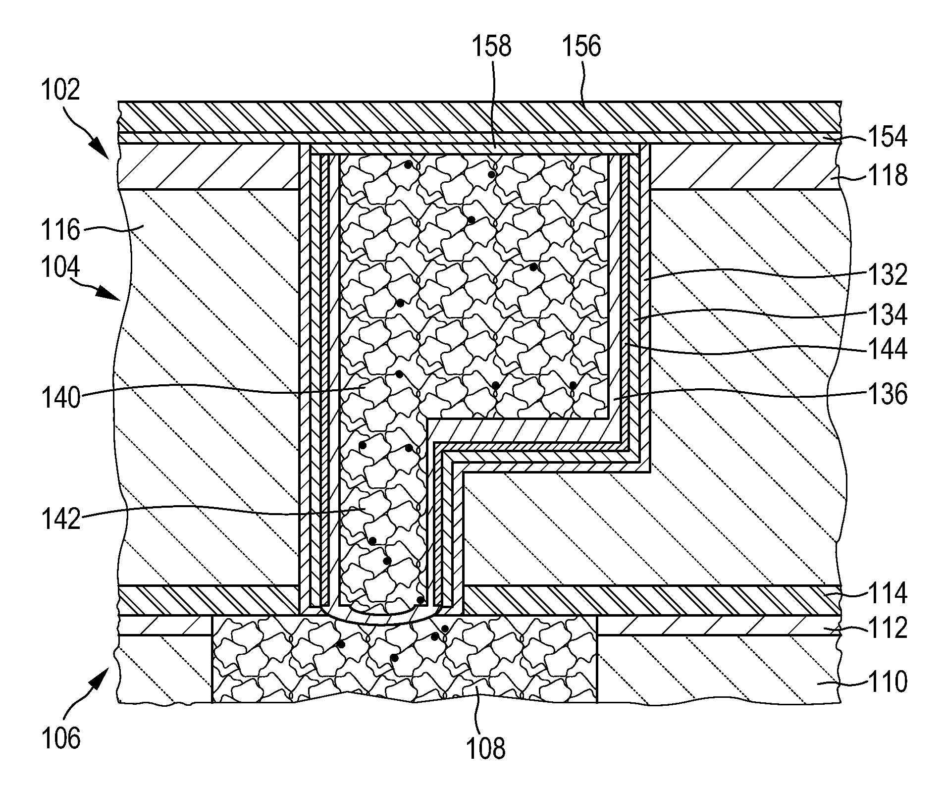
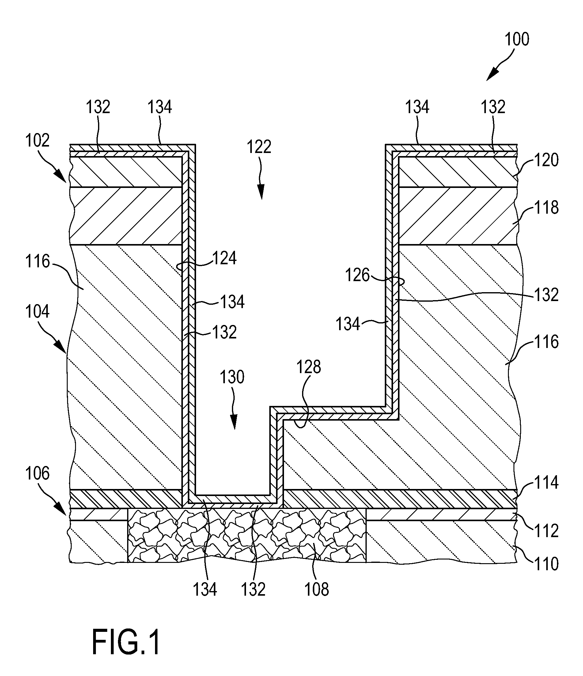
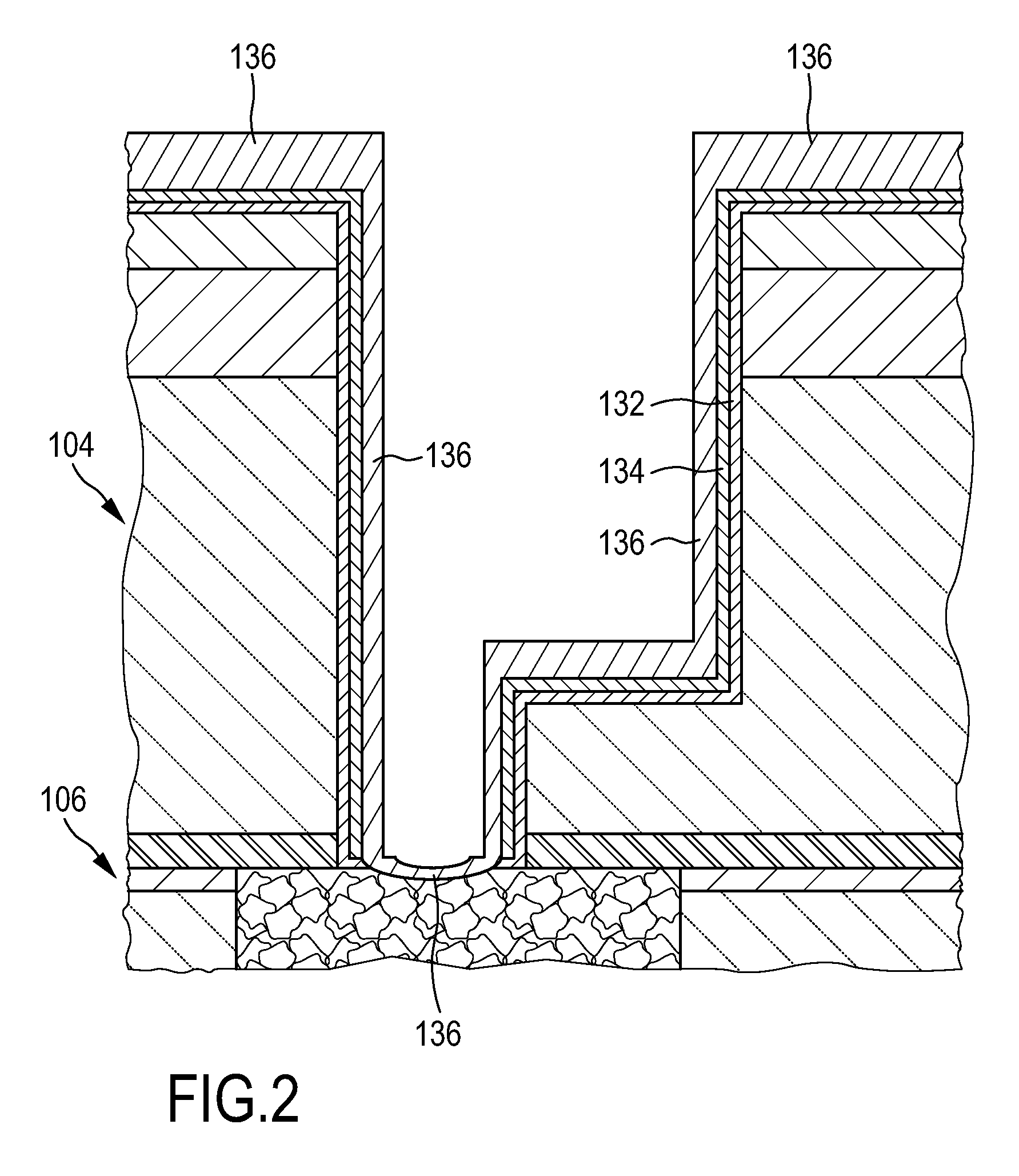
[0043]FIGS. 1-8 show an interconnect element of an integrated-circuit 100 device in a schematic cross-sectional view during different stages of its fabrication.

[0044]The schematic cross-sectional view of FIGS. 1-8 focuses on a section of an interconnect stack 102 of the integrated-circuit device. The section shown forms a part of a metal level 104 on top of an underlying metal level 106. As an illustrative example, metal level 104 could form a third metal level of the interconnect stack 102, and metal level 106 could form the second metal level of the interconnect stack 102.

[0045]At the processing stage shown in FIG. 1 the underlying metal level 106 has been completed and comprises a metal interconnect element 108, which is laterally embedded in a dielectric layer 110. Note that in FIG. 1 the cross-section of metal level 106 is represented in a simplified manner. The structure of metal level 104 can be used on all metal levels. However, it is also possible to use sidewall barriers t...


PUM

PropertyMeasurementUnit
thicknessaaaaaaaaaa
thicknessaaaaaaaaaa
thicknessaaaaaaaaaa

Abstract

The present invention relates to an integrated-circuit device that has at least one Copper-containing feature in a dielectric layer, and a diffusion-barrier layer stack arranged between the feature and the dielectric layer. The integrated-circuit device of the invention has a diffusion-barrier layer stack, which comprises, in a direction from the Copper-containing feature to the dielectric layer, a CuSiN layer and a SiN layer. This layer combination provides an efficient barrier for suppressing Copper diffusion from the feature into the dielectric layer. Furthermore, a CuSiN/SiN layer sequence provides an improved adhesion between the layers of the diffusion-barrier layer stack and the dielectric layer, and thus improves the electromigration performance of the integrated-circuit device during operation. Therefore, the reliability of device operation and the lifetime of the integrate-circuit device are improved in comparison with prior-art devices. The invention further relates to a method for fabricating such an integrated-circuit device.

Description

FIELD OF THE INVENTION[0001]The present invention relates to an integrated-circuit device that has at least one Copper-containing feature in a dielectric layer, and a diffusion-barrier layer stack arranged between the feature and the dielectric layer.BACKGROUND OF THE INVENTION[0002]In the design of integrated-circuit devices, decreasing the resistance-capacitance (RC) delay time in interconnect elements between the circuit elements, such as transistors, is an important goal for increasing the speed of signal transmission between circuit elements. In order to reduce the RC delay time, a known strategy is to use a porous ultra-low-k (P-ULk) insulator material to decrease the capacitance, and to use Copper-containing material for the interconnect elements for providing a low resistance.[0003]The use of Copper in interconnect elements, however, requires the provision of a diffusion barrier between an interconnect element and the neighboring dielectric layer. For keeping the resistance ...

Claims


Application Information

Patent Timeline
Patent Type & Authority Applications(United States)
IPC IPC(8): H01L23/532H01L21/768
CPCH01L21/76831H01L21/76846H01L21/76849H01L21/76855H01L23/53295H01L21/76873H01L21/76877H01L21/76886H01L23/53238H01L21/76867H01L2924/0002H01L2924/00
Inventor JOURDAN, NICOLASGOSSET, LAURANT GEORGESTORRES, JOAQUIN
Owner NXP BV
Why Eureka
Try Eureka