
Method of making silicon carbide semiconductor device

a technology of silicon carbide and semiconductor devices, applied in semiconductor devices, radio frequency controlled devices, electrical apparatus, etc., can solve the problems of insufficient reduction of electric field concentration, difficult alignment between trench gate and p-type deep layer, gate insulating film breakage, etc., and achieve the effect of reducing electric field concentration

Active Publication Date: 2009-11-12
DENSO CORP
View PDF4 Cites 32 Cited by
  • Summary
  • Abstract
  • Description
  • Claims
  • Application Information

AI Technical Summary

Benefits of technology

The present invention provides a method for making a SiC semiconductor device with a structure that reduces electric field concentration in a gate oxide layer formed in a trench. The method ensures that a deep layer is deeper than the trench. The invention also provides a method for making a silicon carbide semiconductor device with an inversion mode MOSFET that includes a current scattering layer and a base region. The technical effects of the invention include reducing electric field concentration, improving the stability and reliability of the semiconductor device, and improving the performance and reliability of the MOSFET.

Problems solved by technology

However, there is a big problem, when the trench-gate structure is applied to SiC.
As a result, it is likely that a breakdown of the gate insulating film occurs at a corner of the trench.
However, the reduction in the electric field concentration is insufficient, and a further reduction is required.
Since alignment between the trench gate and the p-type deep layer is difficult, there may occur a certain amount of variation in a distance from a side wall of the trench gate to the p-type deep layer.
As a result, characteristic variations between products may occur, and yield rates may be low.
In such a structure, when a p-type base region and the p-type deep layer are divided by the n-type current scattering layer, the effect of reducing the electric field concentration may be weakened due to the fact that the p-type deep layer is not fixed to a source potential.
Further, since it is difficult to control the depth of the trench, there is a possibility that the depth of the trench becomes greater than the depth of the p-type deep layer.
However, an enormous amount of energy is required to form the p-type deep layer having a desired depth in a solid material such as SiC.
Therefore, there is a need to prepare an ion implantation apparatus that can perform ion implantation by using an enormous amount of energy.
However, since such an ion implantation apparatus is costly, another approach is required.

Method used


Image

  • Method of making silicon carbide semiconductor device
  • Method of making silicon carbide semiconductor device
  • Method of making silicon carbide semiconductor device

Examples


first embodiment

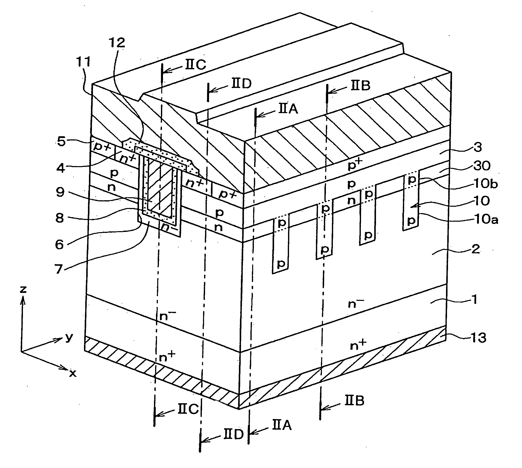
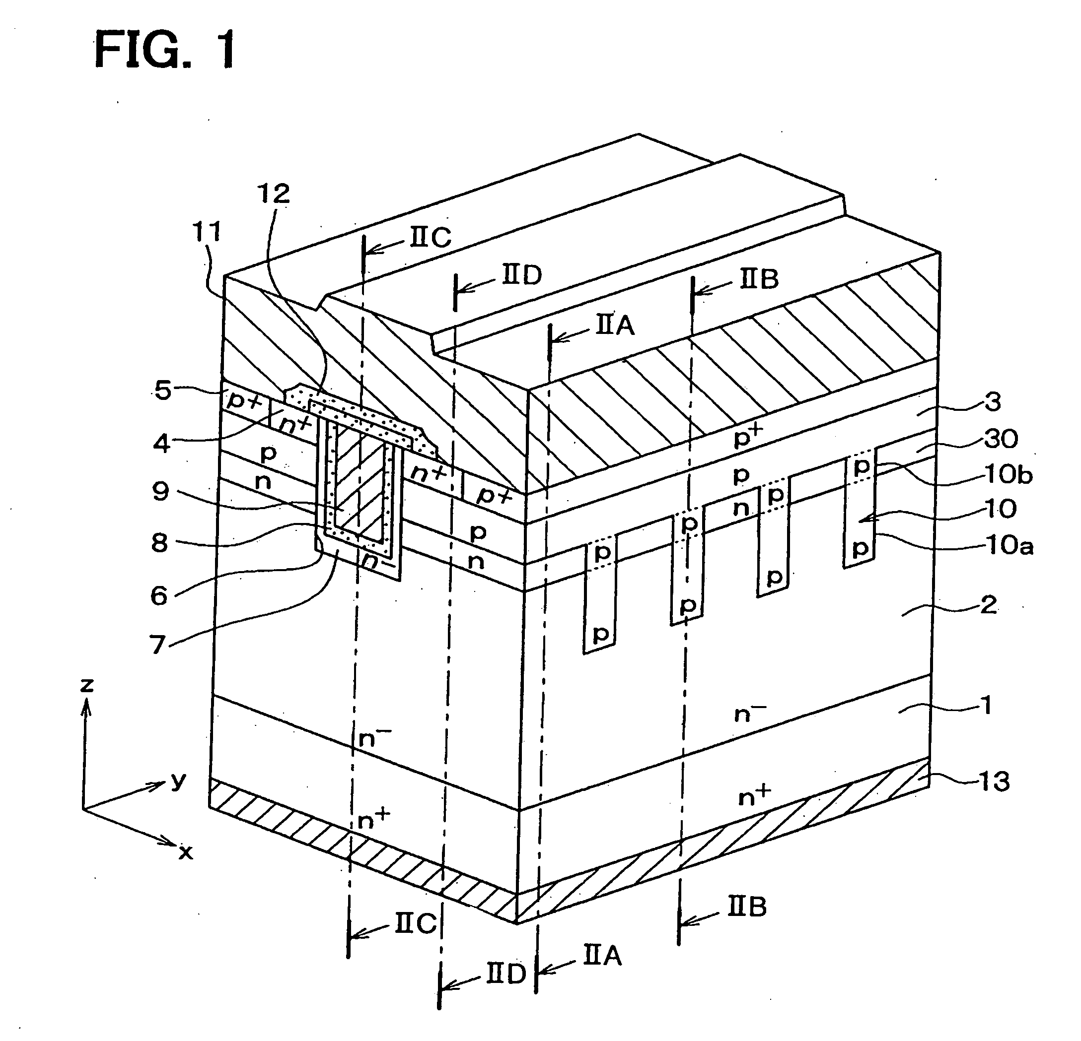
[0030]A first embodiment of the present invention is described. Here, an accumulation-mode trench-gate MOSFET is described as an element provided in a SiC semiconductor device.

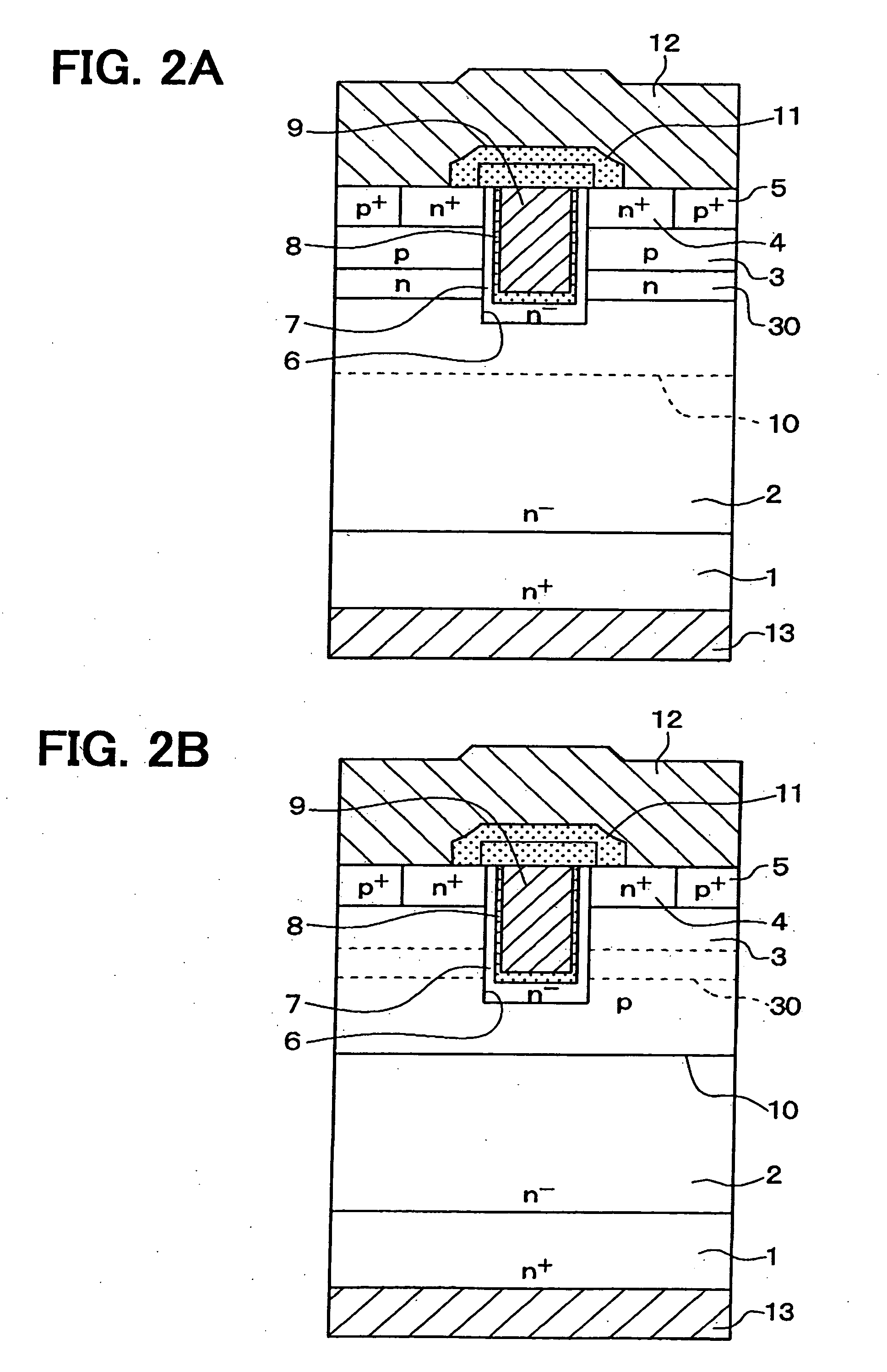
[0031]FIG. 1 is a cross-sectional perspective view of a trench-gate MOSFET according to the present invention. This figure corresponds to one cell of the MOSFET. Although this figure illustrates one cell of the MOSFET, multiple MOSFETs, each of which has the same structure as the MOSFET shown in FIG. 1, are arranged adjacent to each other. FIGS. 2A-2D are diagrams illustrating cross-sectional views of the MOSFET of FIG. 1. FIG. 2A is the cross-sectional view taken along the line IIA-IIA in parallel to the xz plane of FIG. 1. FIG. 2B is the cross-sectional view taken along the line IIB-IIB in parallel to the xz plane of FIG. 1. FIG. 2C is the cross-sectional view taken along the line IIC-IIC in parallel to the yz plane of FIG. 1. FIG. 2D is the cross-sectional view taken along the line IID-IID in parallel to th...

second embodiment

[0074]A second embodiment of the present invention is described. A difference between the first and second embodiments is a relationship between the lower layer 10a and the upper layer 10b of the p-type deep layer 10. Since a basic structure is the same between the first and second embodiments, only the difference is described.

[0075]FIG. 11 is a diagram illustrating a cross-sectional view of a trench-gate MOSFET of a SiC semiconductor device according to the second embodiment. Portions of the second embodiment corresponding to the portions shown in FIG. 1 and FIGS. 2A-2C are almost the same as those of the first embodiment, and a portion of the second embodiment corresponding to the portion shown in FIG. 2D is different than that of the first embodiment. FIG. 11 is a cross-sectional view of the portion corresponding to the portion shown in FIG. 2D.

[0076]As shown in FIG. 11, a separation distance L2 between adjacent upper layers 10b is greater than a separation distance L1 between ad...

third embodiment

[0077]A third embodiment of the present invention is described. A difference between the first and third embodiments is a relationship between the lower layer 10a and the upper layer 10b of the p-type deep layer 10. Since a basic structure is the same between the first and third embodiments, only the difference is described.

[0078]FIG. 12 is a diagram illustrating a cross-sectional view of a trench-gate MOSFET of a SiC semiconductor device according to the third embodiment. Portions of the third embodiment corresponding to the portions shown in FIG. 1 and FIGS. 2A-2C are almost the same as those of the first embodiment, and a portion of the third embodiment corresponding to the portion shown in FIG. 2D is different than that of the first embodiment. FIG. 12 is a cross-sectional view of the portion corresponding to the portion shown in FIG. 2D.

[0079]As shown in FIG. 12, a width W2 of a bottom side of the upper layer 10b is less than a width W1 of the lower layer 10a, and a width W3 of...


PUM


Abstract

In a method of making a silicon carbide semiconductor device having a MOSFET, after a mask is placed on a surface of a first conductivity type drift layer of silicon carbide, ion implantation is performed by using the mask to form a lower layer of a deep layer extending in one direction. A first conductivity type current scattering layer having a higher concentration than the drift layer is formed on the surface of the drift layer. After another mask is placed on a surface of the current scattering layer, ion implantation is performed by using the other mask to form an upper layer of the deep layer at a position corresponding to the lower layer in such a manner that the lower layer and the upper layer are connected together.

Description

CROSS REFERENCE TO RELATED APPLICATION[0001]This application is based on and incorporates herein by reference Japanese Patent Application No. 2008-104606 filed on Apr. 14, 2008.FIELD OF THE INVENTION[0002]The present invention relates to a method of making a silicon carbide (SiC) semiconductor device having a trench gate.BACKGROUND OF THE INVENTION[0003]In recent years, SiC has attracted attention as a material for a power device having high electric field breakdown strength. A SiC semiconductor device can control a large electric current due to its high electric field breakdown strength. Therefore, the SiC semiconductor device is expected to be used to control a motor of a hybrid vehicle.[0004]Increasing channel density is an effective way to allow a larger electric current to flow in a SiC semiconductor device. Therefore, in a silicon transistor, a MOSFET having a trench-gate structure has been adopted and put to practical use. A trench-gate structure can be applied to a SiC semic...

Claims


Application Information

Patent Timeline
Patent Type & Authority Applications(United States)
IPC IPC(8): H01L21/336
CPCH01L29/0623H01L29/0634H01L29/7828H01L29/1608H01L29/66068H01L29/0847
Inventor AKIBA, ATSUYAOKUNO, EIICHI
Owner DENSO CORP
Learn More