High speed orthogonal gate edmos device and fabrication

a technology of orthogonal gate and edmos, which is applied in the direction of semiconductor devices, basic electric elements, electrical appliances, etc., can solve the problems of gate switching loss, gate-to-drain capacitance limitation, and usually limited upper cutoff frequency, so as to minimize gate to drain overlap, minimize and reduce the effect of gate to drain capacitan

Inactive Publication Date: 2009-11-19
ASAHI KASEI ELECTRONICS CO LTD
View PDF3 Cites 77 Cited by
  • Summary
  • Abstract
  • Description
  • Claims
  • Application Information

AI Technical Summary

Benefits of technology

[0010]The orthogonal gate extended drain MOSFET (EDMOS) structure of the invention provides a low gate-to-drain capacitance (CGD) and with fabrication steps that are compatible with the standard CMOS flow. It has an orthogonal gate structure, different from conventional EDMOS transistors. It has a gate electrode that i...

Problems solved by technology

While the power MOSFET is capable of switching at high speeds due to the absence of minority carrier transport, input capacitance limits its performance.
Consequently, the upper cutoff frequency is usually limited by the charging and discharging of this input c...

Method used


Image

  • High speed orthogonal gate edmos device and fabrication
  • High speed orthogonal gate edmos device and fabrication
  • High speed orthogonal gate edmos device and fabrication

Examples


Embodiment Construction

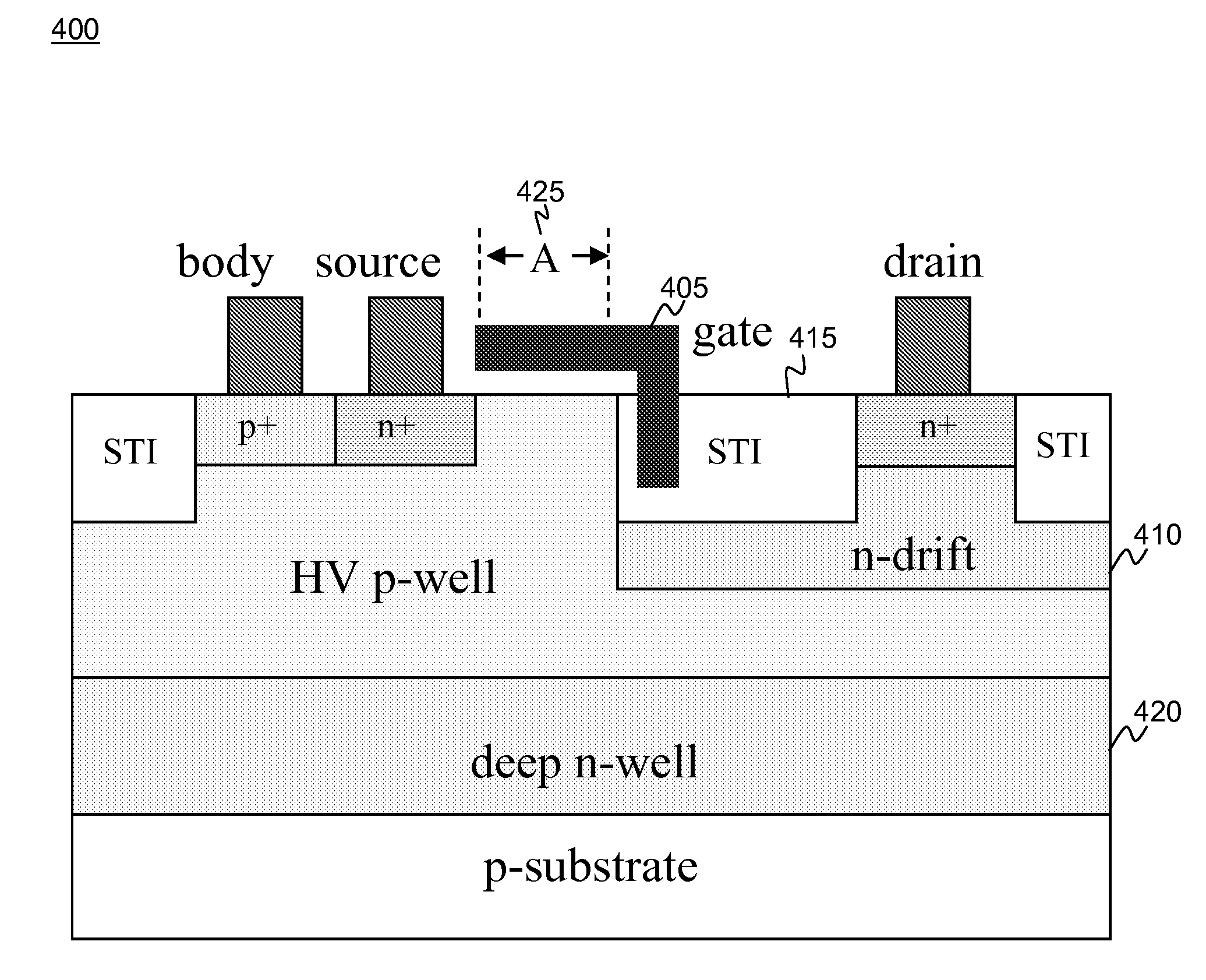
[0026]An orthogonal gate structure replaces the conventional gate / field plate structure in conventional LDMOS or EDMOS transistors. This gate structure reduces the gate-to-drain capacitance, CGD (Miller capacitance). The Figure-of-Merit, gate charge times on-resistance, (Qg×Ron) is improved at least 53%. The dv / dt capability is at least four times higher than that of the conventional EDMOS with similar device structure. The structure is also compatible with standard CMOS fabrication processes that include shallow trench isolation (STI).

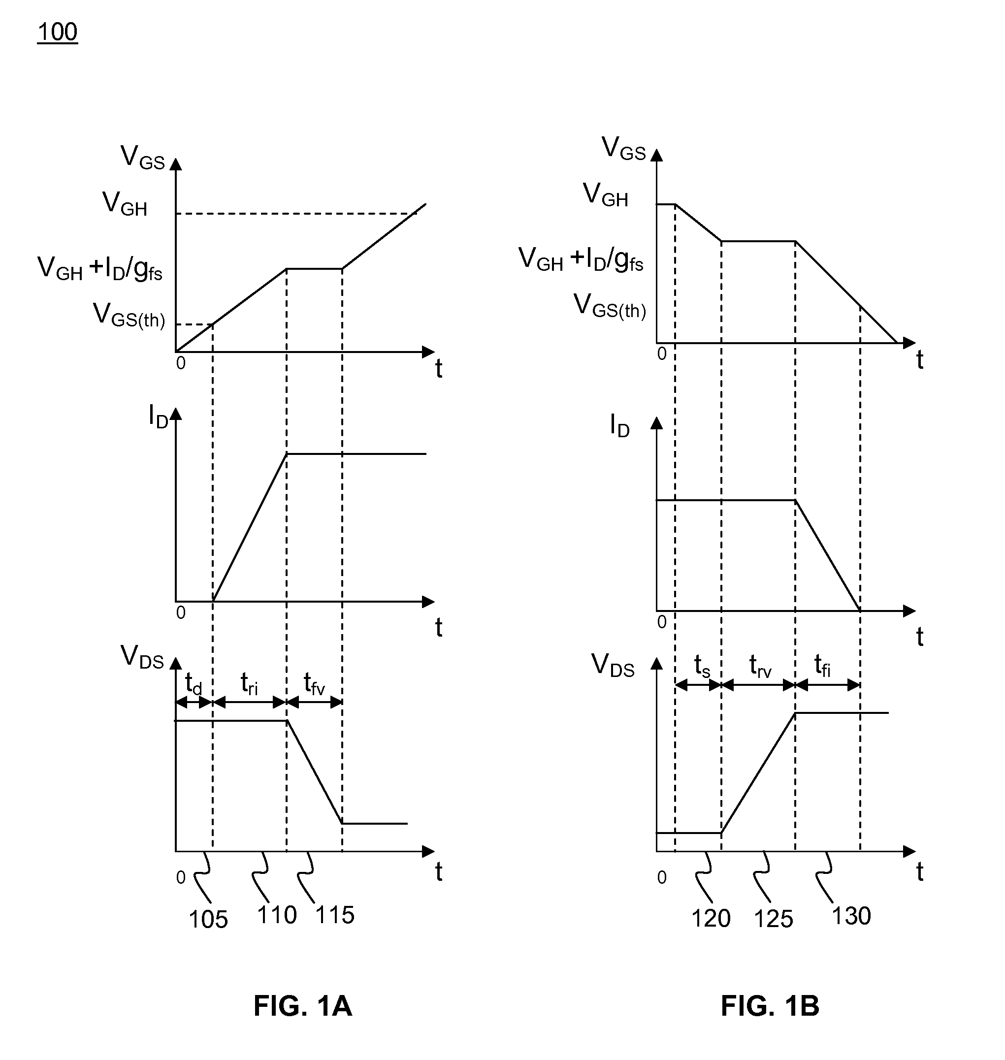
[0027]FIGS. 1A and 1B show simplified graphs 100 of MOS turn-on and off waveforms, respectively. Turn-on delay, ton, is the time taken to charge the input capacitance of the device before drain current conduction can start. Similarly, turn-off delay, toff, is the time taken to discharge the capacitance after the device switched off. The turn-on delay time ton is equal to the sum of td 105, tri 110, and tfv 115 as below and depicted in FIG. 1A.

ton=td+t...


PUM


Abstract

An orthogonal gate extended drain MOSFET (EDMOS) structure provides a low gate-to-drain capacitance (CGD) and exhibits increased reliability. It has a gate electrode that is folded into the shallow trench isolation (STI) oxide region. Horizontal and vertical gate electrode segments provide gate control. It accommodates both high voltage devices and standard CMOS components on the same substrate. Reduced surface field (RESURF) technology is employed to optimize tradeoffs between high breakdown voltage and specific on-resistance. Device fabrication steps are compatible with standard CMOS flow and process modules can be added or removed from baseline CMOS technology.

Description

RELATED APPLICATIONS[0001]This application claims the benefit of U.S. Provisional Application No. 61 / 053,830, filed May 16, 2008; this application is herein incorporated in its entirety by reference.FIELD OF THE INVENTION[0002]The invention relates to power metal-oxide-semiconductor field-effect transistors (MOSFETs). Currently, Lateral Double Diffused MOS (LDMOS) or Extended Drain MOS (EDMOS) transistors are required to switch quickly between “on” and “off” states. In order to accomplish this, the gate to drain overlap capacitance must be minimized. In addition, this will also reduce the gate drive loss as the gate terminal is charged and discharged during every switching cycle.BACKGROUND OF THE INVENTION[0003]Power metal-oxide-semiconductor field-effect transistors (MOSFETs) are used in power electronic circuits as high frequency switches where they alternate between the on- and off-states. This enables the control of high load power with minimal dissipation in the device. While t...

Claims


Application Information

Patent Timeline
IPC IPC(8): H01L29/78H01L21/336
CPCH01L29/0653H01L29/1083H01L29/407H01L29/7835H01L29/42376H01L29/66621H01L29/66659H01L29/4236
Inventor WANG, HAONG, WAI TUNGXU, HUAPING
Owner ASAHI KASEI ELECTRONICS CO LTD
Why Eureka
Try Eureka