

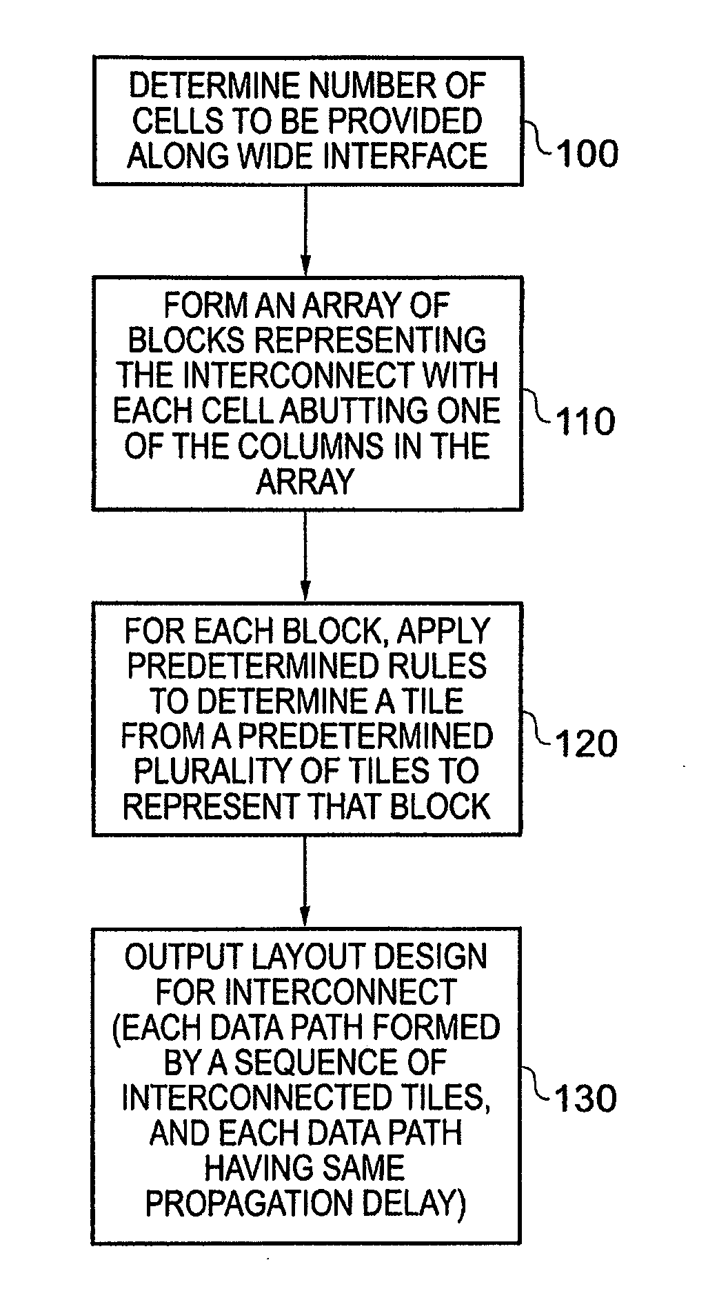
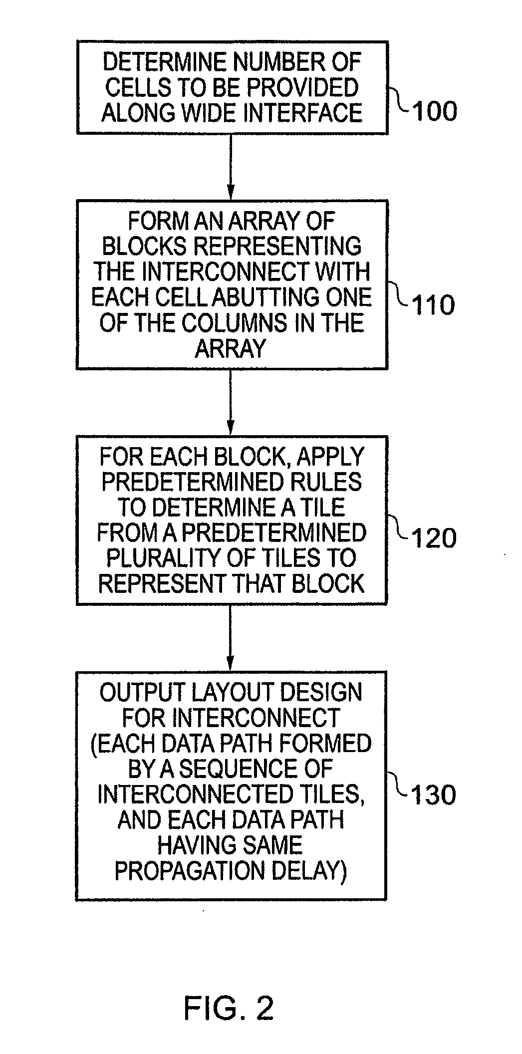
Method, system and computer program product for determining routing of data paths in interconnect circuitry
- Summary
- Abstract
- Description
- Claims
- Application Information
AI Technical Summary
Benefits of technology
Problems solved by technology
Method used
Image

Examples
Embodiment Construction
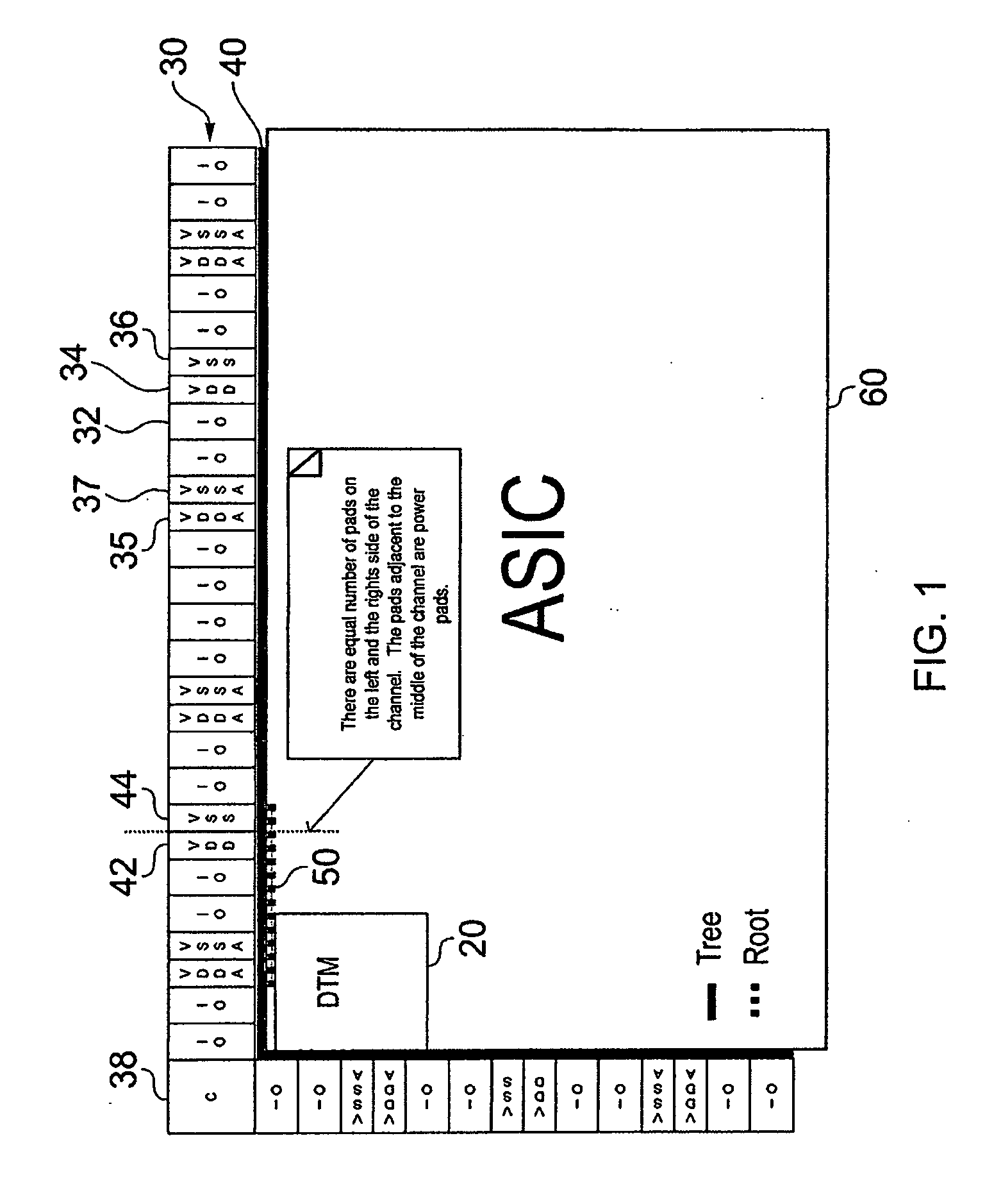
[0057]FIG. 1 is an illustrative example of an integrated circuit 60 incorporating an interconnect circuit 40 designed using the techniques of embodiment of the present invention.
[0058]As shown in FIG. 1, a plurality of devices / components spanning two sides of the integrated circuit 60 are connected to a device 20 within the integrated circuit via the interconnect circuitry 40. The devices 30 include devices which require connection to the device 20 via the interconnect circuitry 40, in FIG. 1 these devices being labelled as IO (input / output) devices, and also may include one or more devices which do not require connection to the device 20. In FIG. 1 the power supply components “VDD”34, “VDDA”35, “VSS”36 and “VSSA”37 are examples of such components which do not require connection to the device 20. A corner element 38 may also be provided at the junction between two linear distribution paths of devices.
[0059]The interconnect circuitry 40 provides a wide interface to the distributed de...
PUM
 Abstract
Description
Claims
Application Information