

Organic light emitting diode display
a light-emitting diode and organic technology, applied in the field of organic light-emitting diodes (oled) display, can solve the problems of disadvantageous multi-layered protective layer on the subpixel in a mass production aspect, and inconvenient multi-layered protective layer in mass production and life span
- Summary
- Abstract
- Description
- Claims
- Application Information
AI Technical Summary
Benefits of technology
Problems solved by technology
Method used
Image

Examples
first exemplary embodiment
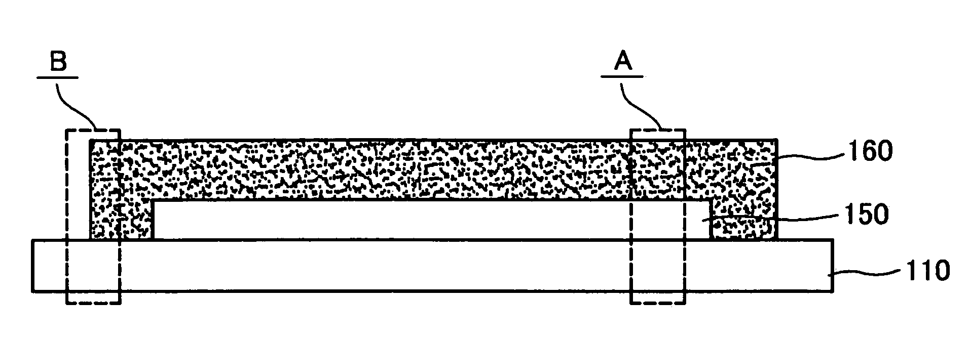
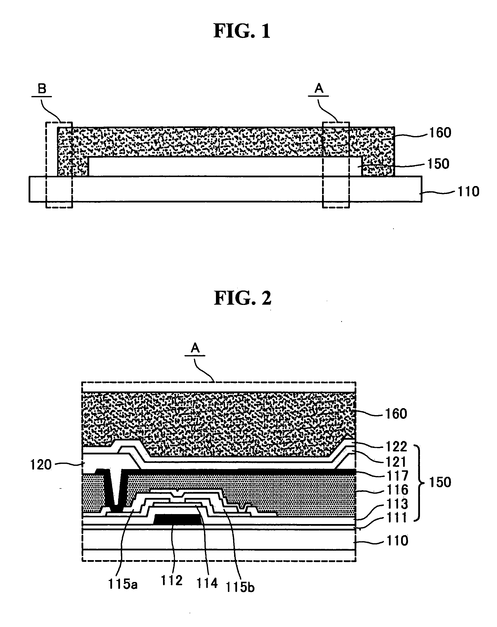
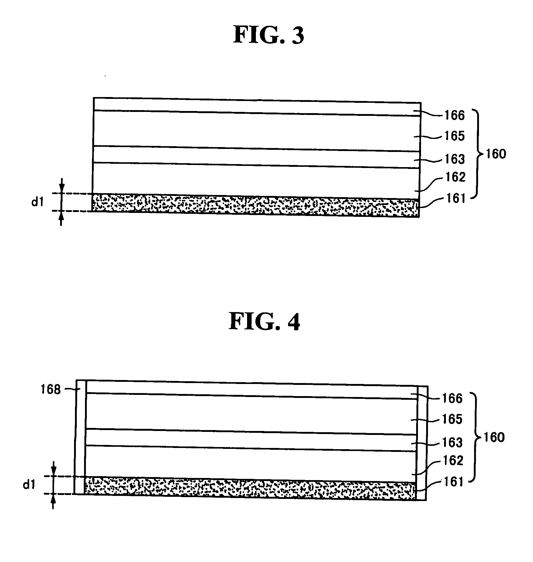
[0035]As shown in FIG. 1, an organic light emitting diode (OLED) display according to a first exemplary embodiment of the invention may include a substrate 110, a subpixel 150 on the substrate 110, and a multi-layered protective layer 160 covering the subpixel 150. The multi-layered protective layer 160 may have a structure in which organic layers and inorganic layers are alternately stacked in a repeated manner and at least one moisture absorbing layer is interposed in the multi-layered protective layer 160.
[0036]The substrate 110 may be formed of a material that has mechanical strength or excellent dimensional stability for forming elements. The substrate 110 may be a glass substrate, a metal substrate, a ceramic substrate, or a plastic substrate. The plastic substrate may be formed of polycarbonate resin, acrylic resin, vinyl chloride resin, polyethyleneterephthalate resin, polyimide resin, polyester resin, epoxy resin, silicon resin, and fluorine resin. Other materials may be us...
second exemplary embodiment
[0063]As shown in FIG. 6, an OLED display according to a second exemplary embodiment of the invention may include a substrate 210, a subpixel 250 on the substrate 210, and a multi-layered protective layer 260 covering the subpixel 250. The multi-layered protective layer 260 may have a structure in which organic layers and inorganic layers are alternately stacked in a repeated manner and at least one moisture absorbing layer is interposed in the multi-layered protective layer 260.
[0064]The substrate 210 may be formed of a material that has mechanical strength or excellent dimensional stability for forming elements. The substrate 210 may be a glass substrate, a metal substrate, a ceramic substrate, or a plastic substrate. The plastic substrate may be formed of polycarbonate resin, acrylic resin, vinyl chloride resin, polyethyleneterephthalate resin, polyimide resin, polyester resin, epoxy resin, silicon resin, and fluorine resin. Other materials may be used for the substrate 210.
[0065...
third exemplary embodiment
[0093]As shown in FIG. 11, an OLED display according to a third exemplary embodiment of the invention may include a substrate 310, a subpixel 350 on the substrate 310, and a multi-layered protective layer 360 covering the subpixel 350. The multi-layered protective layer 360 may have a structure in which at least one moisture absorbing layer is interposed between inorganic layers.
[0094]The subpixel 350 may include a transistor including a switching transistor, a drive transistor, and a capacitor and an organic light emitting diode on the transistor.
[0095]Since a structure of the subpixel 350 shown in FIG. 12 is substantially the same as the subpixel 150 shown in FIG. 2, a further description may be briefly made or may be entirely omitted. The multi-layered protective layer 360 is positioned on the subpixel 350 to cover the subpixel 350.
[0096]The multi-layered protective layer 360 is described in detail below with reference to FIGS. 13 and 14.
[0097]As shown in FIG. 13, the multi-layer...
PUM
 Abstract
Description
Claims
Application Information