Semiconductor packages having electromagnetic interference-shielding function, manufacturing method thereof and jig

a technology of electromagnetic interference shielding and semiconductors, applied in the direction of electrolysis components, vacuum evaporation coatings, coatings, etc., can solve the problems of affecting the operation of other electronic equipment, so as to achieve low manufacturing costs

Inactive Publication Date: 2009-12-03
YOON JUM CHAE
View PDF7 Cites 42 Cited by
  • Summary
  • Abstract
  • Description
  • Claims
  • Application Information

AI Technical Summary

Benefits of technology

[0009]Therefore, the present invention has been made in view of the above problems, and it is an object of the present invention to provide a method for shielding electromagnetic interference (EMI) emitted from the semiconductor package, in which an overall process is very simple and convenient manner and the manufacturing cost is low and which can be applied to various kinds of semiconductor packages.
[0011]Another object of the present invention is to provide a jig for use in a plasma sputtering device which is used to block a portion on which the electromagnetic interference (EMI)-shielding film does not need to be coated in forming the electromagnetic interference (EMI)-shielding film on the surface of the semiconductor package using the plasma sputtering device.

Problems solved by technology

Such electromagnetic radiation acts as electromagnetic interference (EMI) or radio frequency interference (RFI) that hinders the operation of other electronic equipment.
For instance, EMI or RFI causes a problem in that advanced equipment such as an automatic facility system, an aircraft or the like is erroneously operated, stops in its operation, etc.
Such erroneous operation or operation stoppage may cause enormous property damage and even casualties.
However, the above-mentioned package has the disadvantage that the manufacturing cost is raised due to an increase in the number of parts in the case where the metallized cover is fabricated separately, and the assembling work of parts is cumbersome due to additional provision of a process for mounting the metallized cover.
In addition, the conventional package has a limitation that it works against the semiconductor development trend toward miniaturization.
Thus, in the case where it is impossible to immerse the electronic package in the etching solution or the chemical precipitation tank, the plating itself becomes impossible.
In addition, in case of the spraying method, spray efficiency is deteriorated, and a sprayed thickness is thick and non-uniform, which is not suitable for forming a thin film.

Method used


Image

  • Semiconductor packages having electromagnetic interference-shielding function, manufacturing method thereof and jig
  • Semiconductor packages having electromagnetic interference-shielding function, manufacturing method thereof and jig
  • Semiconductor packages having electromagnetic interference-shielding function, manufacturing method thereof and jig

Examples


Embodiment Construction

[0030]Reference will now be made in detail to the embodiments of the present invention, examples of which are illustrated in the accompanying drawings, wherein like reference numerals refer to the like elements throughout.

[0031]In the following description, the detailed description of known function and constructions unnecessarily obscuring the subject matter of the present invention will be avoided hereinafter. Terms to be described later are defined in consideration of functions in the present invention. Therefore, the terms may be changed depending on the intentions of users or administrators, customs or the like. Thus, the definitions should be made based on the entire description of the present invention.

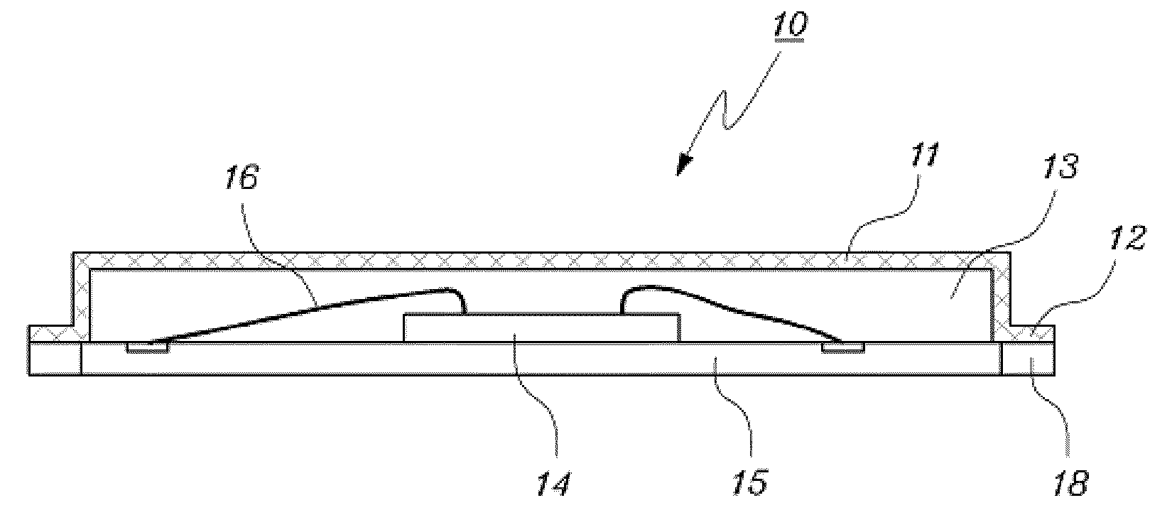
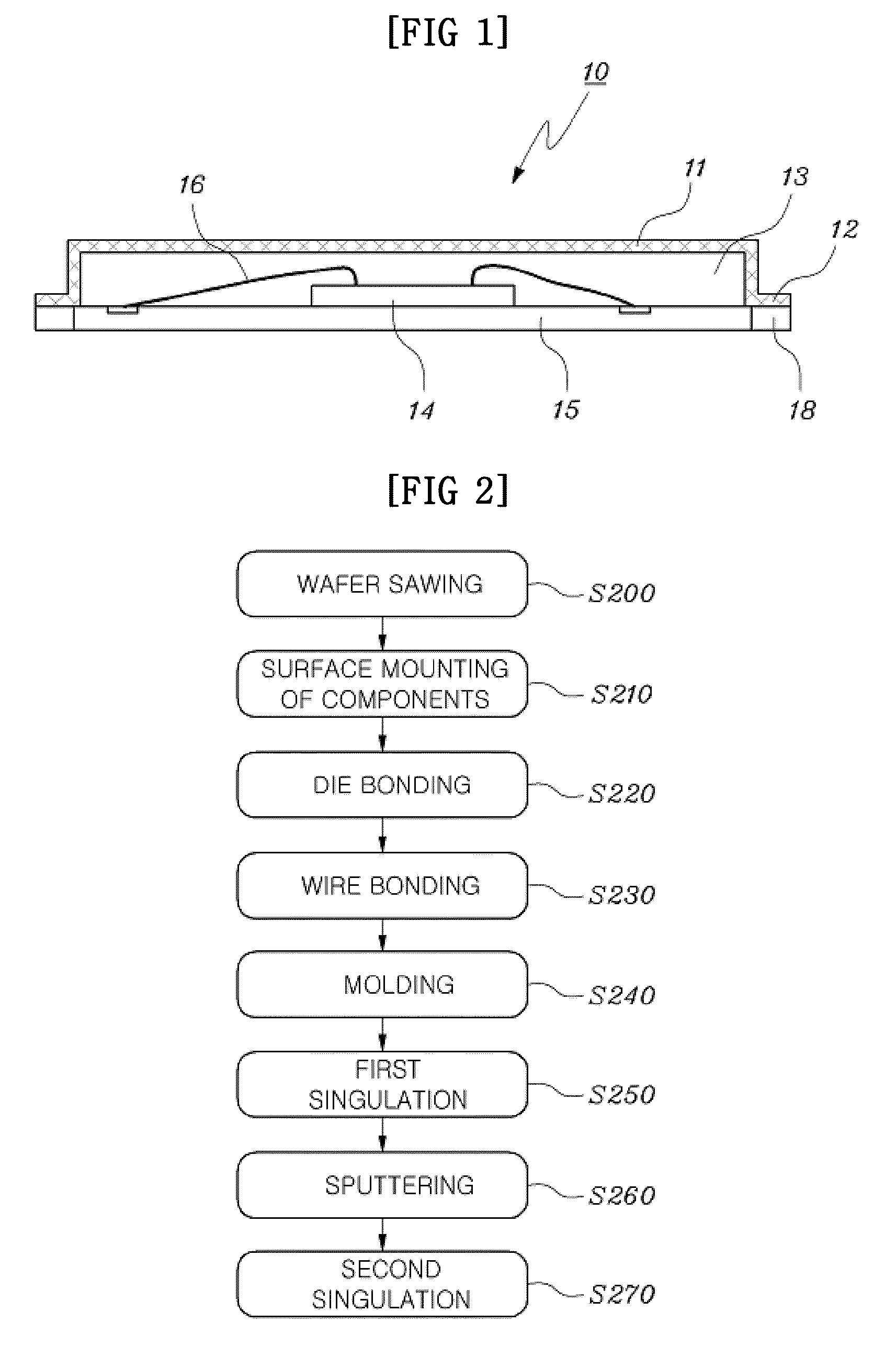
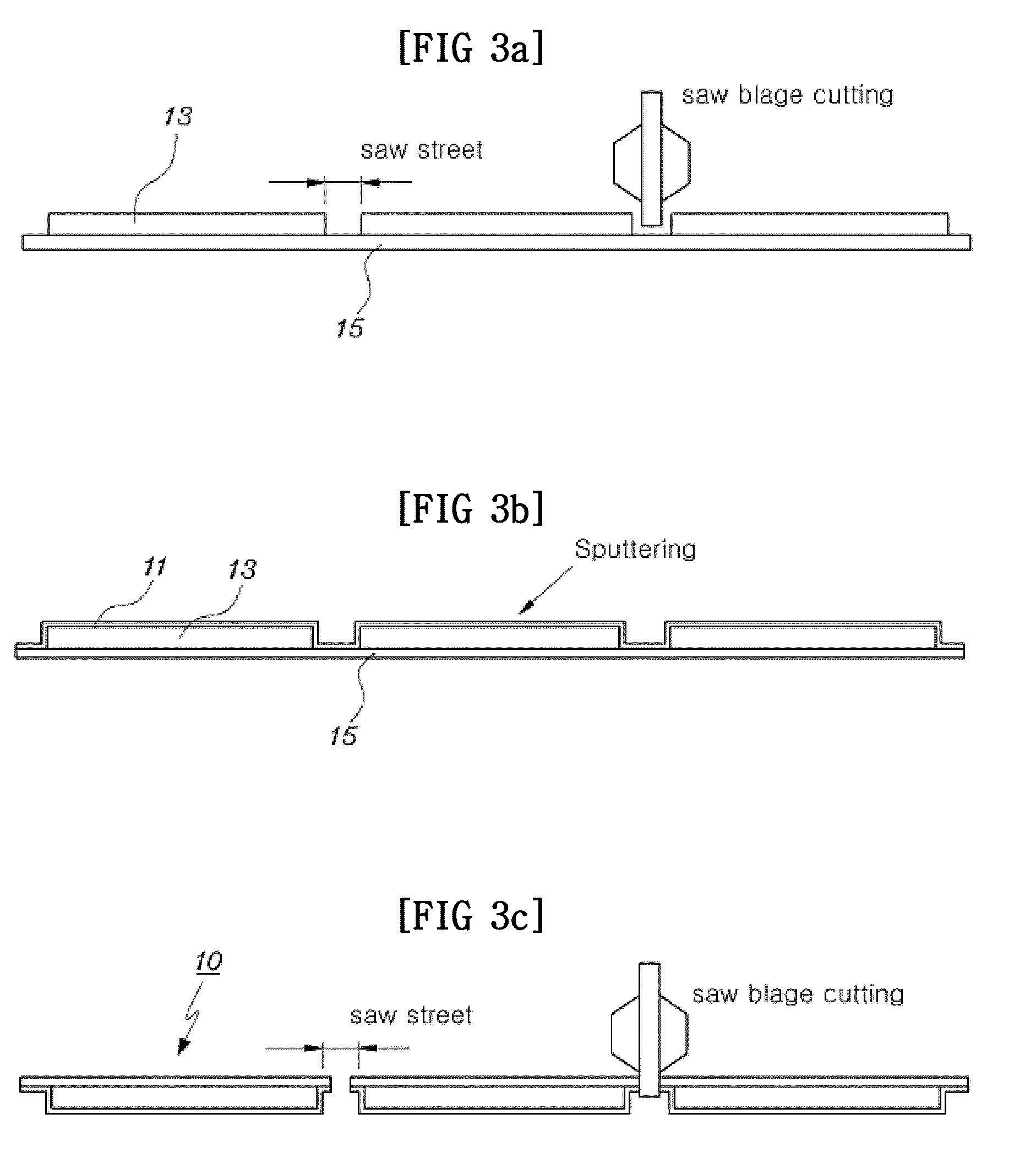
[0032]FIG. 1 is a side cross-sectional view illustrating a semiconductor SIP module package having an electromagnetic interference (EMI)-shielding function according to the present invention, and FIG. 2 is a manufacturing process chart of the semiconductor SIP module package of...


PUM

PropertyMeasurementUnit
timeaaaaaaaaaa
timeaaaaaaaaaa
timeaaaaaaaaaa

Abstract

The present invention relates to relates to a semiconductor package having a function of shielding electromagnetic interference (EMI), a manufacturing method thereof and a jig, and more particularly, to such a semiconductor package having an electromagnetic interference (EMI)-shielding function, a manufacturing method thereof and a jig for use in a plasma sputtering, in which a nickel alloy is coated on the surface of a semiconductor package by a sputtering method so as to shield electromagnetic interference (EMI) generated from the semiconductor package.

Description

BACKGROUND OF THE INVENTION[0001]1. Field of the Invention[0002]The present invention relates to a semiconductor package having a function of shielding electromagnetic interference (EMI), a manufacturing method thereof and a jig, and more particularly, to such a semiconductor package having an electromagnetic interference (EMI)-shielding function, a manufacturing method thereof and a jig for use in a plasma sputtering, in which a nickel alloy is coated on the surface of a semiconductor package by a sputtering method so as to shield electromagnetic interference (EMI) generated from the semiconductor package.[0003]2. Background of the Related Art[0004]Recently, since the development of semiconductors, the semiconductors have been employed in a variety of electronic products such as household electric appliances, industrial equipment, medical equipment, etc. The semiconductor-related technology follows a trend toward miniaturization, lightness and multifunction, and digitalization of t...

Claims


Application Information

Patent Timeline
Patent Type & Authority Applications(United States)
IPC IPC(8): H01L23/552H01L21/78H01L21/60H01L21/56C23C14/00
CPCH01L23/552H01L24/45H01L2924/1461H01L2924/01028H01L2924/01006H01L2924/3025H01L2924/30105H01L2924/16152H01L2924/01082H01L2924/01079H01L2924/01078H01L24/48H01L24/97H01L2224/45124H01L2224/45144H01L2224/48091H01L2224/48227H01L2224/97H01L2924/01004H01L2924/01013H01L2924/01018H01L2924/01027H01L2924/01029H01L2924/01033H01L2924/01047H01L2924/0105H01L2924/00014H01L2224/85H01L2924/00H01L2924/12042H01L23/06
Inventor YOON, JUM-CHAEHYUN, EUN-SOOKIM, SEUNG-KI
Owner YOON JUM CHAE
Why Eureka
Try Eureka