Method and system for model-based design and layout of an integrated circuit

a model-based design and integrated circuit technology, applied in the direction of cad circuit design, program control, instruments, etc., can solve the problems of many ic design failures, ic design manufacturing has gotten steadily more difficult, and feature dimensions vary, so as to achieve the effect of increasing the quantity of data, increasing the complexity of physical and lithographic effects during manufacture, and increasing the amount of resources

Active Publication Date: 2009-12-10
CADENCE DESIGN SYST INC
View PDF26 Cites 28 Cited by
  • Summary
  • Abstract
  • Description
  • Claims
  • Application Information

AI Technical Summary

Benefits of technology

[0011]The problem with this approach is that lithography simulation and RET optimization is very resource intensive, requiring large quantities of both time and computing assets for adequate results. As the quantity of data in modern IC designs become larger and larger over time, the resources required for performing model-based verification and optimization upon these IC designs also becomes much greater. This problem is exacerbated by constantly improving IC manufacturing technologies that can create IC chips at ever-smaller feature sizes, which allows increasingly greater quantities of transistors to be placed within the same chip area, resulting in more complex physical and lithographic effects during manufacture.
[0012]To address these problems, among others, the present invention in some embodiments provides an approach for allowing EDA tools to implement very efficient approaches to allow the tools to directly address the effects of manufacturing processes, e.g., to identify and prevent problems caused by lithography processing. Fast models and pattern checking are employed to integrate lithography and manufacturing aware processes within EDA tools such as routers. In some embodiments, this approach avoids the rigid requirement of conventional tools that rely exclusively upon rule checks, avoiding the need to create overly complex rules that may or may not accurately reflect the real-world manufacturing problems that may occur to the design. This also avoids the need to hardcode the EDA fool (e.g., modify the router software) to explicitly target particular bad patterns, which significantly reduces or eliminates the need to perform this highly manual and error-prone effort. Moreover, this approach in some embodiments can also be used to avoid the very slow process of using external tools to verify the routed design and to provide feedback to the router. In this context, the external tool will often call the problems it finds “hotspots”.

Problems solved by technology

For example, optical distortions during the lithography process may cause variations in feature dimensions (e.g. line widths) that are patterned using masks.
However, certain IC design may actually need parameters that are more or less cautious than other designs.
Since DRC rules typically operate on an “all or nothing” basis, this means that many IC design may fail DRC processing even, though they would function properly for intended purposes if manufactured.
Further, manufacturing an IC design has gotten steadily more difficult, so much so that certain 2D configurations of geometry may not function properly, even though they satisfy all the DRC rules.
As a result, the routed design may contain numerous layout portions that are problematic once manufacturing is performed, and would contribute to yield or functionality problems.
The problem with this approach is that lithography simulation and RET optimization is very resource intensive, requiring large quantities of both time and computing assets for adequate results.
This problem is exacerbated by constantly improving IC manufacturing technologies that can create IC chips at ever-smaller feature sizes, which allows increasingly greater quantities of transistors to be placed within the same chip area, resulting in more complex physical and lithographic effects during manufacture.
In this context, the external tool will often call the problems it finds “hotspots”.

Method used


Image

  • Method and system for model-based design and layout of an integrated circuit
  • Method and system for model-based design and layout of an integrated circuit
  • Method and system for model-based design and layout of an integrated circuit

Examples


Embodiment Construction

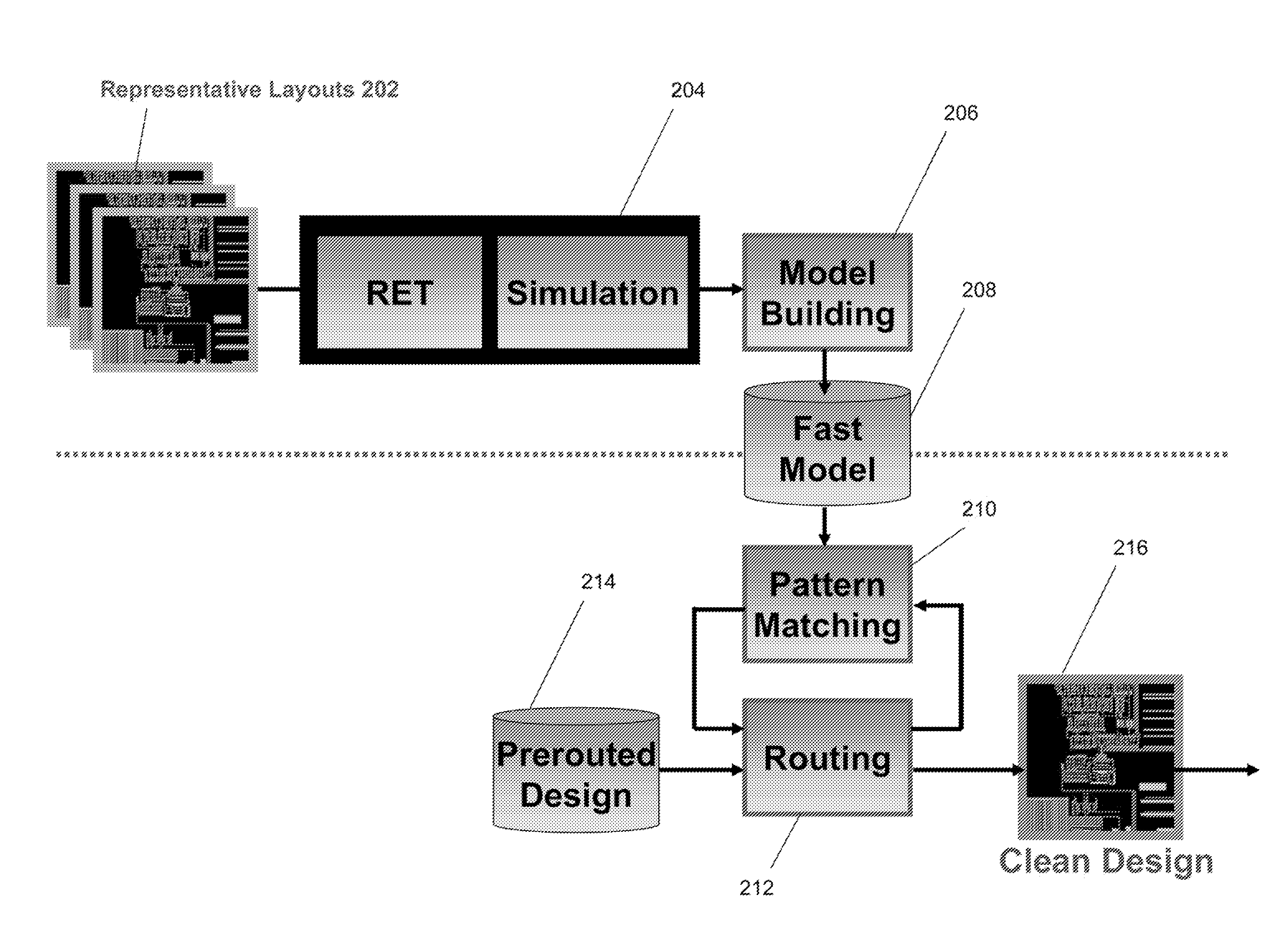
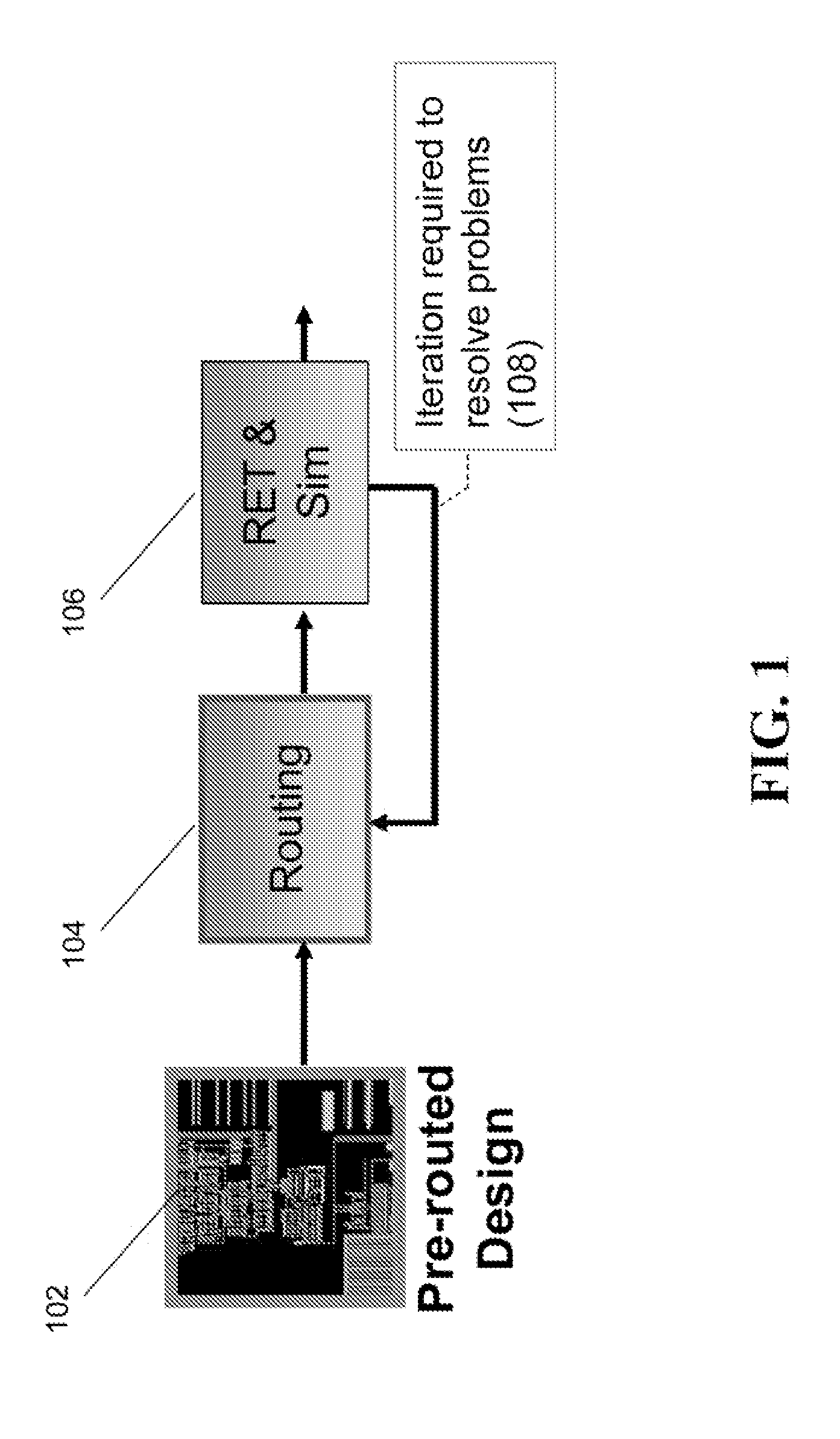
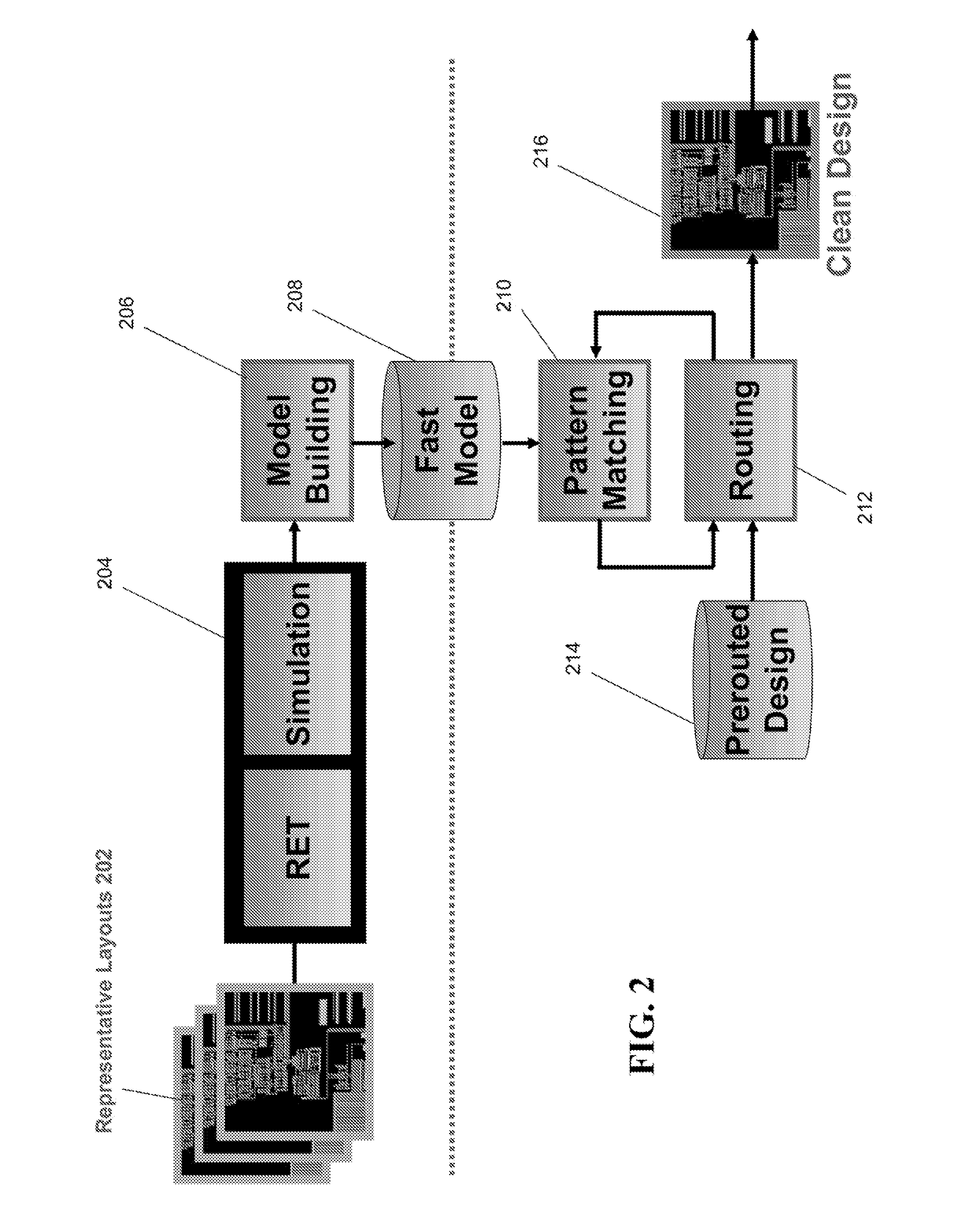
[0021]The present approach is directed to an improved method, system, and computer readable medium for performing routing, full chip flows, and “hotspot” detection. As used herein, the term “hotspot” refers to a portion of a design layout that is identified as corresponding to a manufacturing-related problem, such as may be caused by lithography, chemical metal polishing (CMP), etch, strain, critical area analysis, or any combination thereof. Some embodiments of the invention utilize pattern matching to detect hotspots and to provide lithographically aware routing and chip design, by creating and accessing a bad pattern library. The term “bad pattern”, according to some embodiments, refers to any layout shape or shape pattern that has a negative impact on yield or functionality doe to, for example, lithography, CMP, strain, critical area analysis, and other manufacturing related issues. In this document, the term “hotspot” may be used in certain places synonymously with the term “ba...


PUM


Abstract

A approach is described for allowing electronic design, verification, and optimization tools to implement very efficient approaches to allow the tools to directly address the effects of manufacturing processes, e.g., to identify and prevent problems caused by lithography processing. Fast models and pattern checking are employed to integrate lithography and manufacturing aware processes within EDA tools such as routers.

Description

BACKGROUND AND SUMMARY[0001]The invention is directed to a more efficient approach for hotspot detection, for implementing layout, and for placement, routing, and verification of integrated circuit designs.[0002]A semiconductor integrated circuit (IC) has a large number of electronic components, such as transistors, logic gates, diodes, wires, etc., that are fabricated by forming layers of different materials and of different geometric shapes on various regions of a silicon wafer.[0003]The various components of an integrated circuit are initially defined by their functional, operations and relevant inputs and outputs. From the HDL or other high level description, the actual logic cell implementation is typically determined by logic synthesis, which converts the functional description of the circuit into a specific circuit implementation.[0004]An integrated circuit designer may use a set of EDA application programs to create a physical integrated circuit design layout from a logical ...

Claims


Application Information

Patent Timeline
Patent Type & Authority Applications(United States)
IPC IPC(8): G06F17/50
CPCG06F17/5068G06F30/39
Inventor LAI, YA-CHIEHGENNARI, FRANK E.MOSKEWICZ, MATTHEWDODDI, SRINIVASLEI, JUNJIANGFANG, WEIPINGLAY, KUANGHAO
Owner CADENCE DESIGN SYST INC
Why Eureka
Try Eureka