Efficient light extraction method and device

Active Publication Date: 2009-12-24
LEHIGH UNIVERSITY
View PDF15 Cites 31 Cited by
  • Summary
  • Abstract
  • Description
  • Claims
  • Application Information

AI Technical Summary

Benefits of technology

[0008]A need continues for enhanced, inexpensive and repeatable LED light extraction efficiency.
[0009]The invention provides enhanced and repeatable light emitting device extraction efficiency at a reasonable cost. The invention is describe in an embodiment as a light emitting device comprising at least one p-type layer and at least one n-type layer and a microsphere array surface.
[0010]Also, the invention is a method for improving light efficiency of a light emi

Problems solved by technology

The large index difference makes the reflection quite substantial (per the Fresnel coefficients), and both the Fresnel reflection and critical angle limitations are usually the dominant causes of LED inefficiency.
The disadvantages of surface roughening ar

Method used


Image

  • Efficient light extraction method and device
  • Efficient light extraction method and device
  • Efficient light extraction method and device

Examples


examples

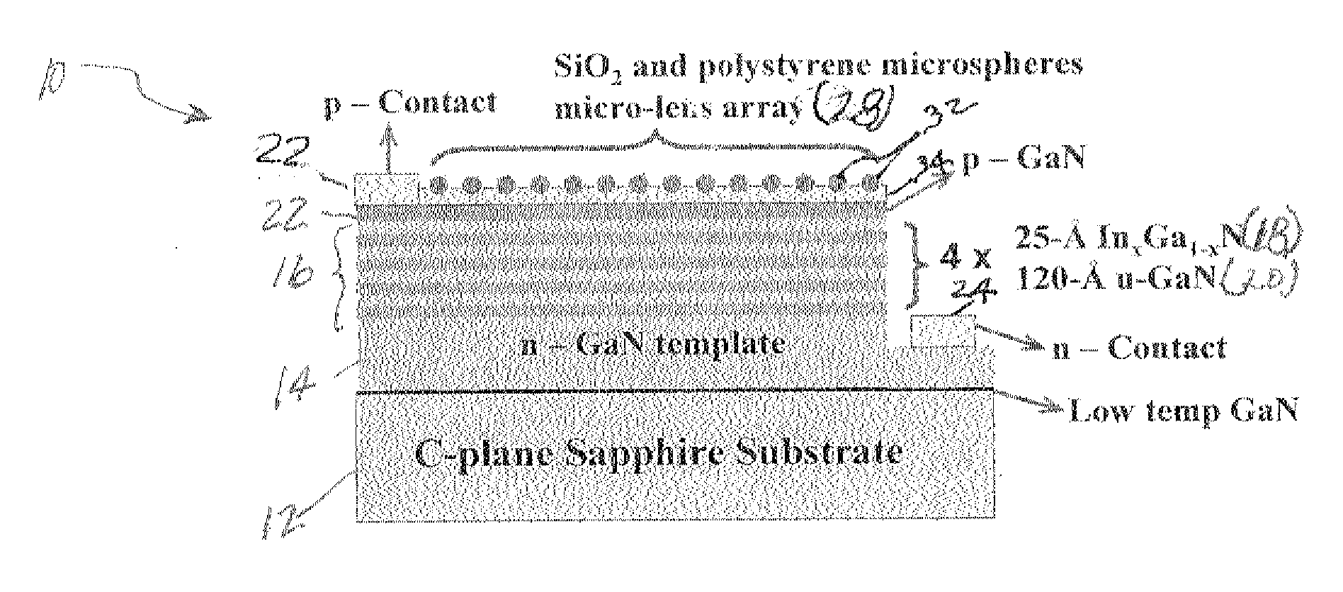
[0035]In these EXAMPLES, a layer of polystyrene (PS) and a monolayer of two-dimensional hexagonal close-packed SiO2 colloidal crystal were deposited on a top surface of an InGaN QW-based device. FIG. 1 illustrates the LED device 10 including a 3-μm GaN template 14 (grown at 1080° C.) on c-plane sapphire substrate 12 using a low-pressure vertical-type MOCVD system, employing a low temperature buffer layer of 30-nm GaN (grown at 535° C.). Active region 16 of the device structure comprised 4-period 2.5-nm InGaN QWs 18 and 12-nm GaN barriers 20. The device 10 included p-GaN layer 22, n-contact 24 and p-contact 26 as shown.

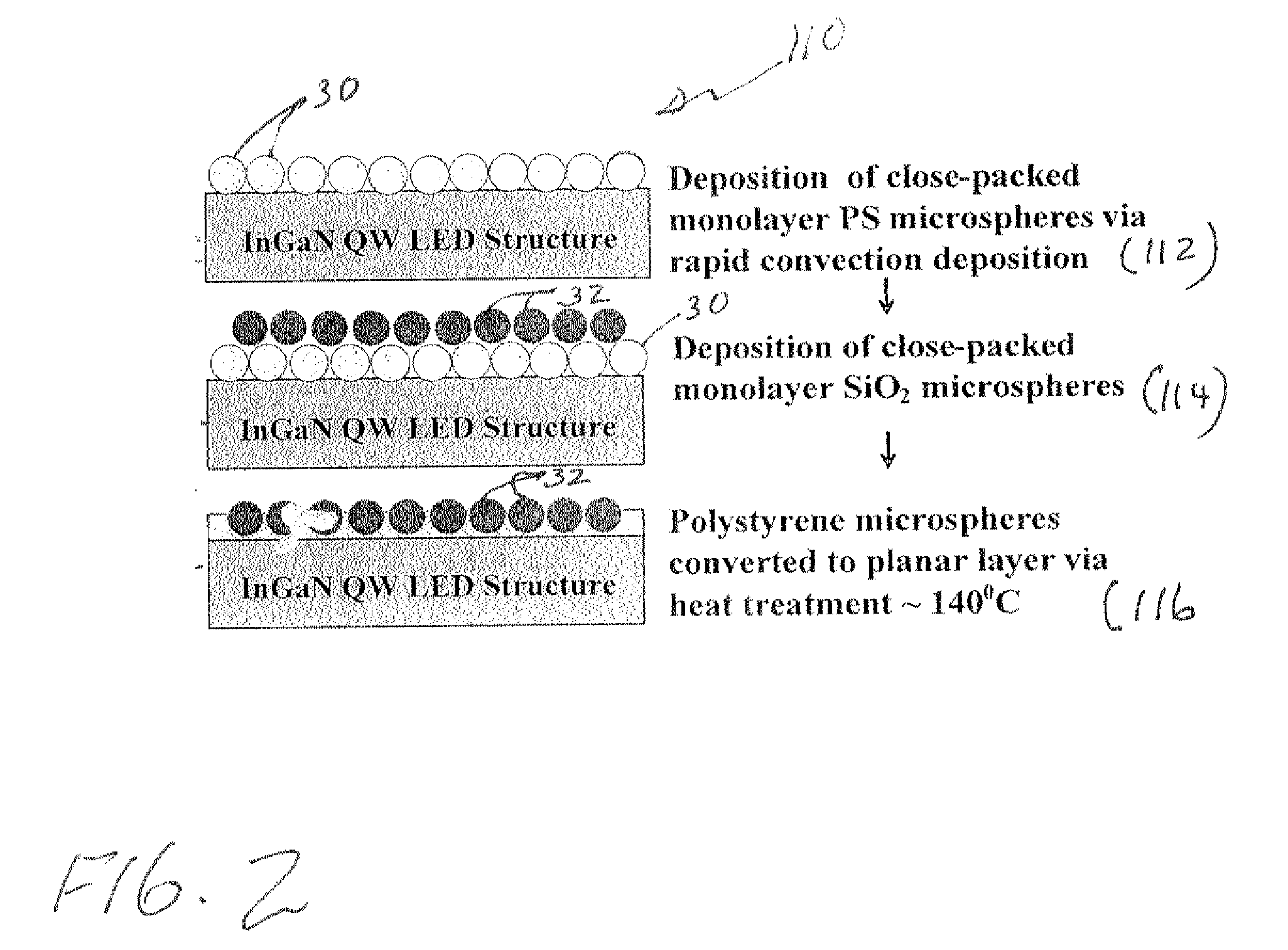
[0036]The LED device 10 included a microlens array surface 28 comprising SiO2 microspheres 32 imbedded in a polystyrene monolayer film 34 prepared In accordance with the process illustrated in FIG. 2. The SiO2 microspheres 32 with diameter of 1.0 μm were semi-buried in the PS film 34, thereby forming a close-packed lens-like array 28. The refractive index of GaN in the...


PUM


Abstract

A tight emitting device comprises at least one p-type layer and at least one n-type layer and a microlens array surface. A method for improving light efficiency of a light emitting device, comprises depositing polystyrene microspheres by rapid convection deposition on surface of light emitting device; depositing a monolayer of close-packed SIO2 microspheres onto the polystyrene microspheres; and heal treating to convert the polystyrene microspheres into a planar microlayer film to provide a surface comprising substantially two-dimensional (2D) hexagonal close-packed S1O2 colloidal microsphere crystals partially imposed into a polystyrene monolayer film.

Description

CROSS REFERENCE TO RELATED APPLICATION[0001]This application claims the benefit of U.S. Provisional Application No. 60871823, filed 24 Dec. 2006, which is incorporated herein by reference.[0002]This invention was made with government support under Contracts Nos. ______ respectively awarded by the Department of Defense—Army Research Lab and by the National Science Foundation. The government has certain rights in the invention.BACKGROUND OF THE INVENTION[0003]The invention relates to a light emitting device, particularly to an improved light extraction efficiency method and light emitting diode (LED).[0004]A light-emitting diode is a semiconductor diode that emits incoherent narrow-spectrum light when electrically biased in the forward direction of a p-n junction. This effect is a form of electroluminescence.[0005]An LED typically comprises a small area source, often with extra optics added to the chip that shapes its radiation pattern. Color of emitted light depends on semiconductor ...

Claims


Application Information

Patent Timeline
IPC IPC(8): H01L33/00H01L33/22H01L33/44
CPCB82Y20/00H01L33/44H01L33/22
Inventor TANSU, NELSONEE, YIK KHOONGILCHRIST, JAMES F.KUMNORKAEW, PISITARIF, RONALD A.
Owner LEHIGH UNIVERSITY
Why Eureka
Try Eureka