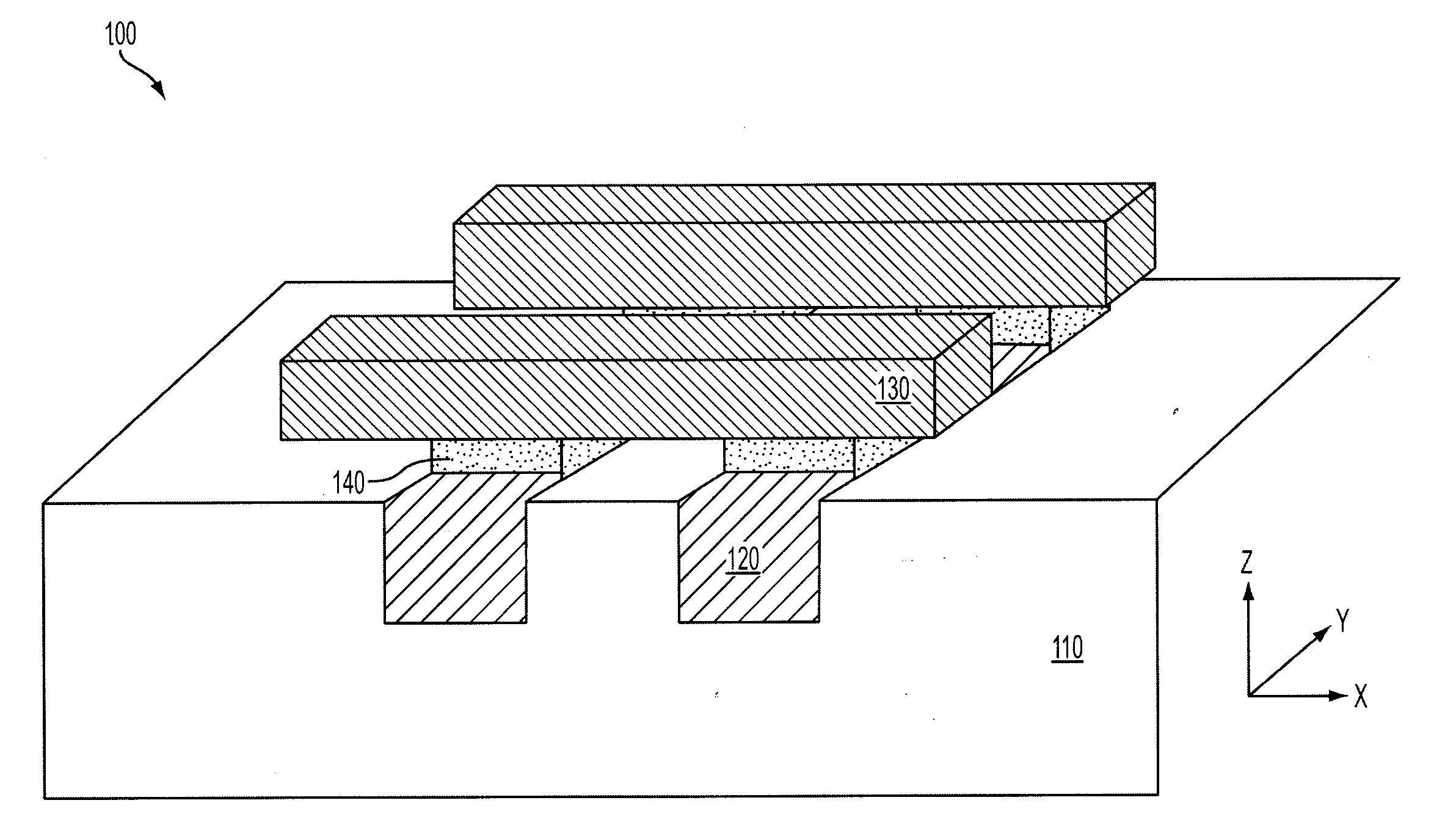
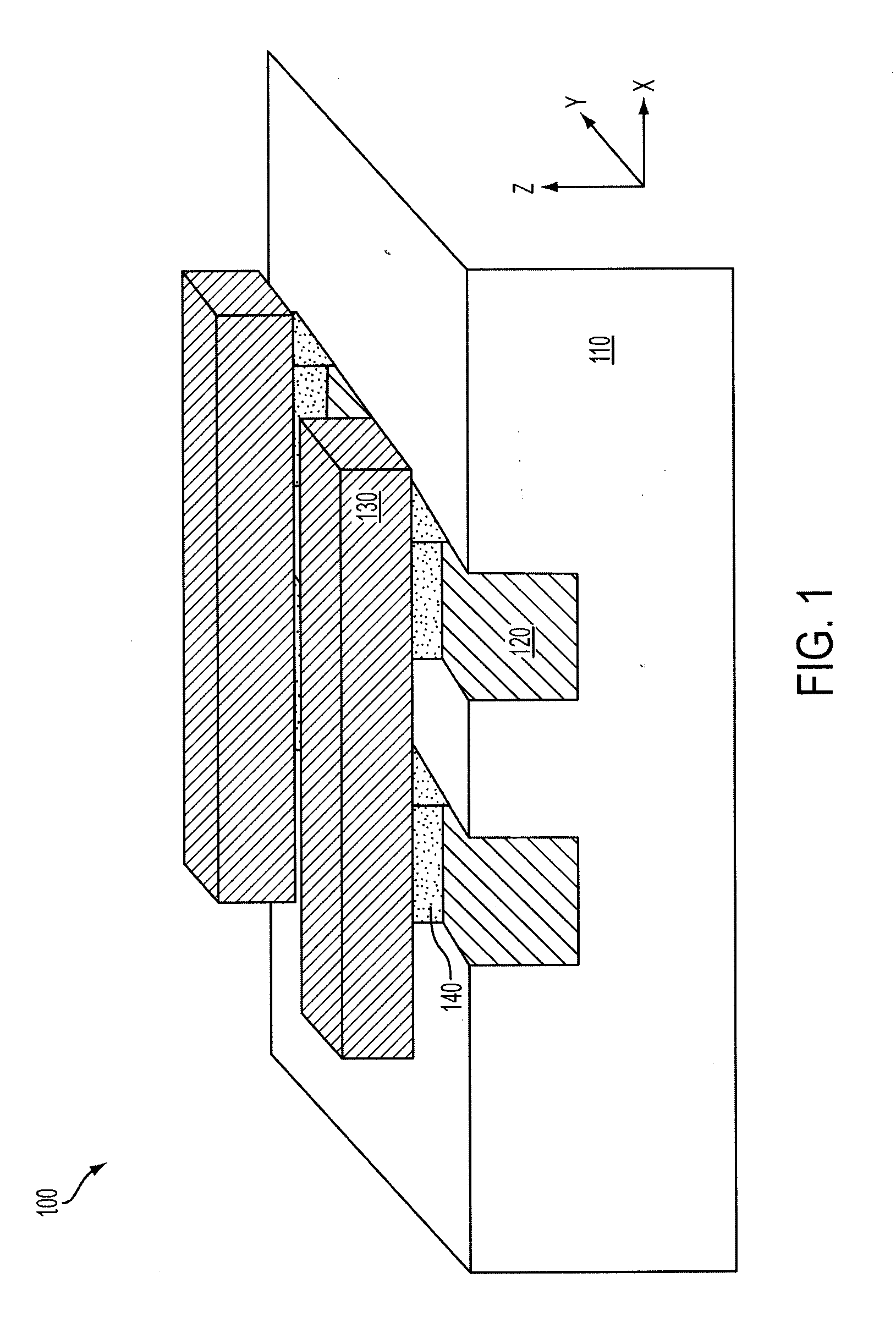
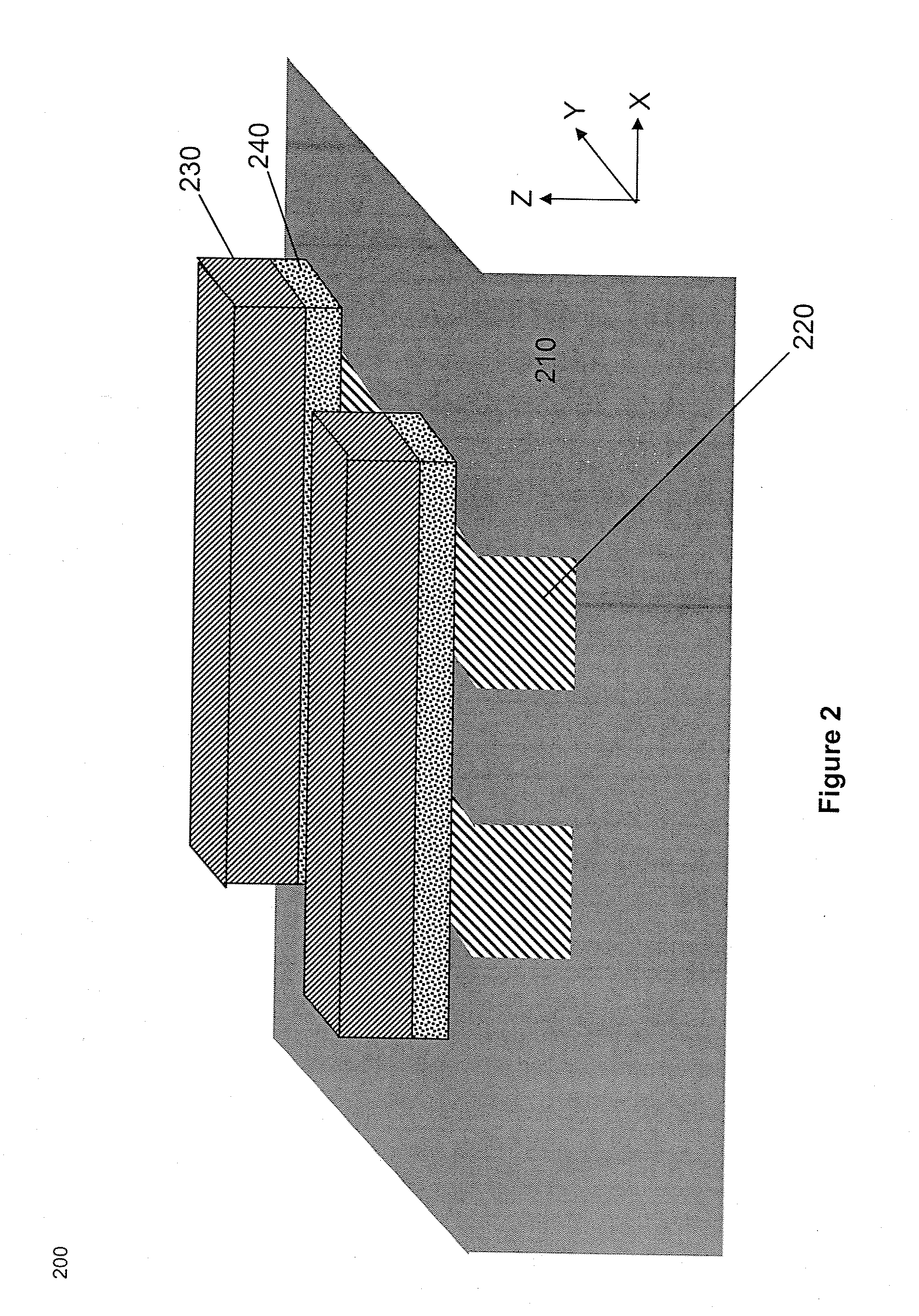
[0038]One or more embodiments include one or more of the following features. The nanotube article comprises a plurality of nanotube blocks, each block corresponding to a memory cell, each block programmable with an informational state. The nanotube article comprises a plurality of nanotube traces and each reference line is substantially conformally disposed over and aligned with a corresponding nanotube trace. A region of each nanotube trace corresponds to a memory cell, the region programmable with said informational state. The nanotube article comprises a nanotube plane disposed over the word lines and the bit lines corresponding to the plurality of memory cells. Each reference line includes a trace conformally disposed over a portion of the nanotube plane such that each of a plurality of regions of the nanotube plane corresponding to the plurality of memory cells is programmable with an information state. The reference line comprises a conductor plane disposed over and conformally to the nanotube plane and a plurality of regions of the nanotube plane corresponding to the plurality of memory cells is each programmable with said information state. For each memory cell, the region is the portion of the nanotube plane disposed over the corresponding first electrode.
[0039]One or more embodiments include one or more of the following features. The first and second informational states are nonvolatile. The resistance of the relatively high resistance state is several times greater than the relatively low resistance state. The array further includes a cell selection circuit for each memory cell, the cell selection circuit electrically interposed between the first electrode and the bit line. The cell selection circuit includes a transistor with a gate, a source, and a drain, and wherein the gate is in electrical contact with the first word line, the source is in electrical contact with the first electrode, and the drain is in electrical contact with the bit line. The operation circuit reads an informational state of the memory cell by activating one of the bit line and the word line and applying a read stimulus to the bit line.
[0040]One or more embodiments include one or more of the following features. The first electrode comprises at least one of metallic carbon nanotubes, Ti, TiN, Al, Ta, TaN, Cu, Ru, RuO, Pd, Co, CoSix, Ni, NiSix, TiSix, Si, Pt, PtSix, Au, Ag, and combinations thereof. An intermediate resistance of the nanotube article corresponds to a third informational state of the memory cell. The nanotube article is disposed over the bit lines. The bit lines are disposed over the nanotube article.
[0041]Under another aspect, a method of making a memory array includes providing a plurality of bit lines and word lines and providing a plurality of first electrodes, each first electrode in communication with a bit line and each corresponding to a memory cell. The method includes forming a nanotube fabric over and in electrical communication with the first electrodes, the nanotube fabric comprising a network of unaligned nanotubes, and providing a reference article over and in electrical communication with the nanotube fabric. The method includes providing a memory operation circuit in electrical communication with the bit line, the word line, and the reference article to activate one or more selected memory cells. The operation circuit includes circuitry to program an informational state in at least a portion of the nanotube fabric by applying electrical stimulus to at least one of the bit line, word line, and reference article, in which said electrical stimulus changes the resistance of at least a portion of the nanotube fabric between the first electrode and reference article. A relatively high resistance in said portion of the nanotube fabric corresponds to a first informational state of the memory cell in the array. A relatively low resistance of the nanotube article corresponds to a second informational state of the memory cell in the array.
[0042]One or more embodiments include one or more of the following features. Each bit line and each word line is patterned to have a width of F and wherein the memory array has a density of 6F2. A selected portion of the memory array is active and a selected portion of the memory array is inactive. The inactive portion of the memory array includes memory cells in which an informational state is not programmed into corresponding portions of the nanotube fabric. The patterned reference article comprises a plurality of reference lines, the reference lines substantially parallel to either the bit lines or the word lines. The patterned reference article comprises a reference electrode plane carrying a single reference voltage. The method further includes patterning the nanotube fabric and the reference article to form conductor-on-nanotube traces. The conductor-on-nanotube traces are substantially parallel to either the bit lines or the word lines. The method further includes patterning the nanotube fabric into a plurality of nanotube blocks, each nanotube block corresponding to a memory cell. The method further includes embedding the first electrodes and the nanotube fabric in an insulating substrate. Providing a plurality of first electrodes includes forming a plurality of semiconductor devices, the first electrodes being one node of the semiconductor devices. The semiconductor devices are MOS access devices. The semiconductor devices are select diodes.
[0043]One or more embodiments include one or more of the following features. The nanotube fabric is disposed over the bit lines. The bit lines are disposed over the nanotube fabric. A protective material is applied over an external surface of the nanotube fabric to protect the nanotube fabric during one or more fabrication steps, the protective material comprising at least one of silicon dioxide, silicon nitride, hafnium oxide, zirconium oxide, and aluminum oxide, amorphous silicon, W, Al, Ti, TiN, Ta, spin-on-glasses (SOGs), thermally decomposed polymers, and photoresists. Forming the nanotube fabric further includes forming a nanoparticle layer, the nanoparticle layer selected to adjust the resistance of at least a portion of the nanotube fabric between the first electrode and reference article. The nanoparticle layer comprises at least one of amorphous carbon, alumina, bismuth, cadmium, selenide, gallium nitride, gold, gallium phosphide, germanium, silicon, indium phosphide, magnesium oxide, manganese oxide, nickel, palladium, silicon carbide, titanium, zinc oxide, and silicon germanium.


