Method of manufacturing semiconductor laser

a manufacturing method and laser technology, applied in the direction of lasers, semiconductor devices, semiconductor lasers, etc., can solve the problems of ridge semiconductor lasers being especially susceptible to such stress, change in optical characteristics, and stress in the layer, so as to reduce the efficiency of semiconductor lasers, increase the thickness of insulating films, and reduce the effect of efficiency

Inactive Publication Date: 2010-01-07
MITSUBISHI ELECTRIC CORP
View PDF4 Cites 3 Cited by
  • Summary
  • Abstract
  • Description
  • Claims
  • Application Information

AI Technical Summary

Benefits of technology

[0006]Further, in ridge semiconductor lasers, the generated light is confined within the waveguide by utilizing the difference in refractive index between the ridge and the portions of the semiconductor layer on both sides of the ridge. Therefore, the active layer and the insulating film are separated from each other by a very small distance (approximately 0.3 μm) on both sides of the ridge. As a result, light generated in the active layer leaks into the insulating film, and a portion of the leaked light reaches the electrode on the insulating film and is absorbed therein, resulting in reduced efficiency of the semiconductor laser. To avoid this, the insulating film between the semiconductor layer and the electrode may be increased in thickness. However, an increase in the thickness of the insulating film results in an increase in the distortion of the active layer due to the difference in coefficient of thermal expansion between the semiconductor layer and the insulating film.
[0007]One way to reduce the stress in the semiconductor layer, or active layer, due to the insulating film thereon is to form the insulating film by plasma CVD, etc. However, this causes plasma damage to the active layer, thereby degrading the reliability of the semiconductor laser.
[0008]The present invention has been devised to solve the above problems. It is, therefore, an object of the present invention to provide a method of manufacturing a semiconductor laser having high efficiency and reliability.
[0010]Thus, the present invention enables the manufacture of a semiconductor laser having high efficiency and reliability.

Problems solved by technology

Therefore, forming an insulating film or electrode on a semiconductor layer causes stress in the layer.
Ridge semiconductor lasers are especially susceptible to such stress, since in these lasers the active layer is located near the insulating film.
That is, the active layer is distorted due to the stress, resulting in a change in the optical characteristics and causing crystal defects.
This has been a factor which has limited the reliability of ridge semiconductor lasers.
As a result, light generated in the active layer leaks into the insulating film, and a portion of the leaked light reaches the electrode on the insulating film and is absorbed therein, resulting in reduced efficiency of the semiconductor laser.
However, an increase in the thickness of the insulating film results in an increase in the distortion of the active layer due to the difference in coefficient of thermal expansion between the semiconductor layer and the insulating film.
However, this causes plasma damage to the active layer, thereby degrading the reliability of the semiconductor laser.

Method used


Image

  • Method of manufacturing semiconductor laser
  • Method of manufacturing semiconductor laser
  • Method of manufacturing semiconductor laser

Examples


first embodiment

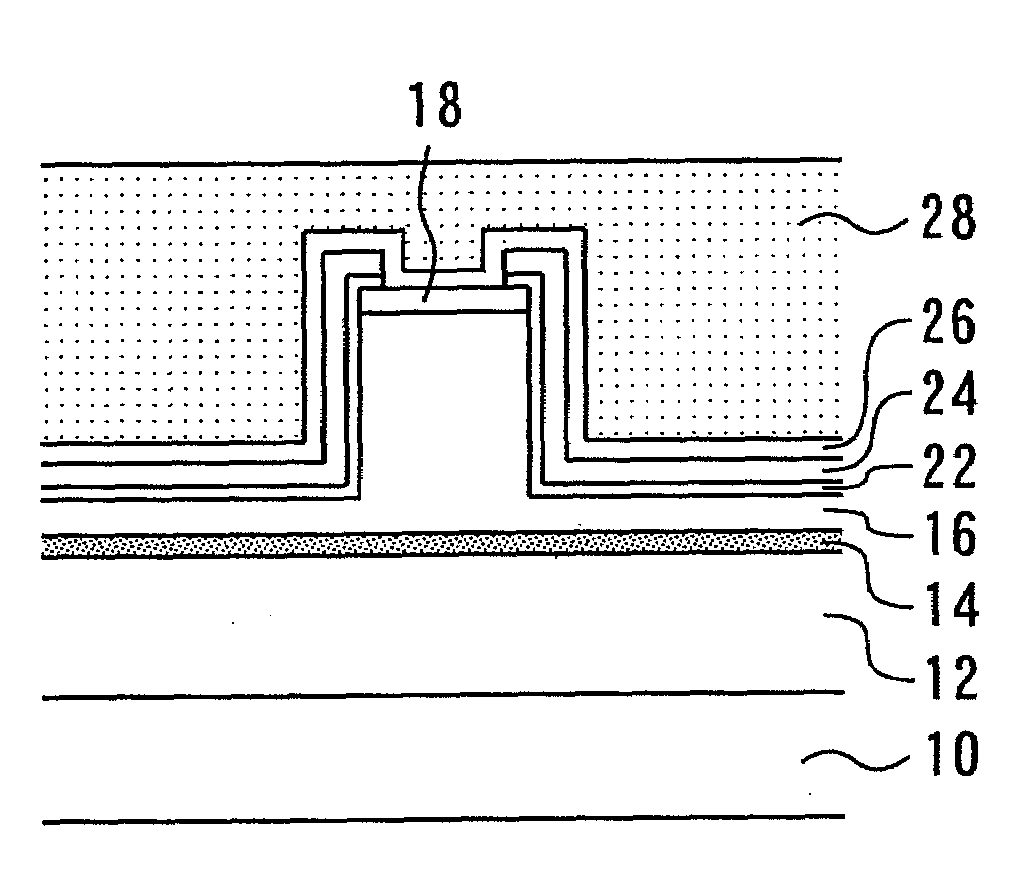
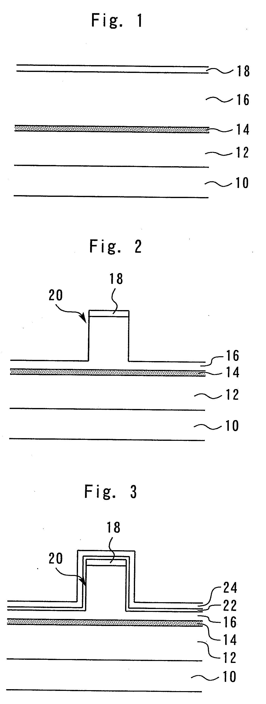
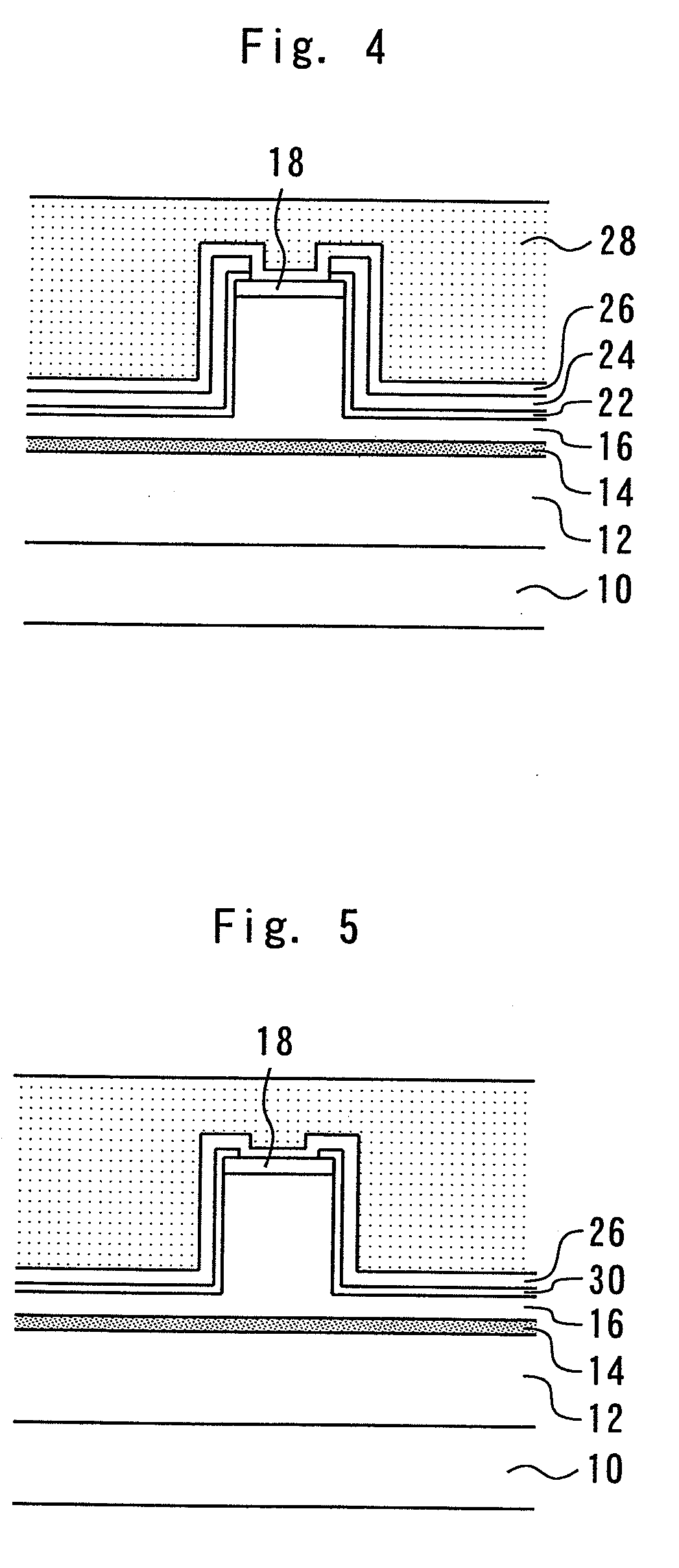
[0022]There will be described, with reference to accompanying drawings, a method of manufacturing a semiconductor laser according to a first embodiment of the present invention.

[0023]First, an n-type cladding layer 12 (serving as a first conductivity type semiconductor layer), an active layer 14, a p-type cladding layer 16 (serving as a second conductivity type semiconductor layer), and a contact layer 18 are sequentially formed on top of one another on a GaAs substrate 10 (serving as a semiconductor substrate), as shown in FIG. 1. Next, a ridge 20 is formed in the p-type cladding layer 16 by means of photolithography and dry etching, as shown in FIG. 2.

[0024]An SiN film 22 (serving as a first insulating film) is then formed on the p-type cladding layer 16 to a thickness of 50 nm by thermal CVD at a temperature of approximately 600° C., as shown in FIG. 3. An SiN film 24 (serving as a second insulating film) is then formed on the SiN film 22 to a thickness of 100 nm by plasma CVD at...

second embodiment

[0033]There will be described, with reference to accompanying drawings, a method of manufacturing a semiconductor laser according to a second embodiment of the present invention. It should be noted that components corresponding to those of the first embodiment bear the same reference numerals and will not be further described (unless necessary).

[0034]First, an n-type cladding layer 12, an active layer 14, a p-type cladding layer 16, and a contact layer 18 are sequentially formed on top of one another on a GaAs substrate 10, and then a ridge 20 is formed in the p-type cladding layer 16, as in the first embodiment.

[0035]Next, an SiN film 22 is formed over the entire surface of the p-type cladding layer 16, as shown in FIG. 7. An SiN film 24 is then formed on the SiN film 22 in such a manner that the SiN film 24 covers only a central region 36 of the resonator, as shown in FIG. 8. It should be noted that the SiN film 24 is formed at lower temperature than the SiN film 22. Subsequently,...

third embodiment

[0037]There will be described, with reference to accompanying drawings, a method of manufacturing a semiconductor laser according to a third embodiment of the present invention. It should be noted that components corresponding to those of the first embodiment bear the same reference numerals and will not be further described (unless necessary).

[0038]First, an n-type cladding layer 12, an active layer 14, a p-type cladding layer 16, and a contact layer 18 are sequentially formed on top of one another on a GaAs substrate 10, and then a ridge 20 is formed in the p-type cladding layer 16, as in the first embodiment.

[0039]Next, an SiN film 32 (serving as an insulating film) is formed on the p-type cladding layer 16 by thermal CVD at a temperature of approximately 600° C., as shown in FIG. 9.

[0040]Etching using a fluorine-containing gas is then performed to thin the SiN film 32 on end regions 34 of the resonator to a thickness of 100 nm or less, as shown in FIG. 10 (the end regions 34 of ...


PUM


Abstract

A method of manufacturing a semiconductor laser includes sequentially forming a first conductivity type semiconductor layer, an active layer, and a second conductivity type semiconductor layer on top of one another on a semiconductor substrate; forming a ridge in the second conductivity type semiconductor layer; forming a first insulating film on the second conductivity type semiconductor layer at a first temperature; forming a second insulating film on the first insulating film at a second temperature, lower than the first temperature; and forming an electrode on the second insulating film.

Description

BACKGROUND OF THE INVENTION[0001]1. Field of the Invention[0002]The present invention relates to a method of manufacturing a semiconductor laser in which an insulating film covers the semiconductor layer having the ridge formed therein, and more particularly to a method of manufacturing such a semiconductor laser having high efficiency and reliability.[0003]2. Background Art[0004]There has been a great need to increase the output and the functionality and reduce the cost of semiconductor lasers for use in optical disc systems. In response to this need, the following method has been used to manufacture a semiconductor laser. First, a first conductivity type semiconductor layer, an active layer, and a second conductivity type semiconductor layer are sequentially formed on top of one another on a semiconductor substrate. Next, a ridge is formed in the second conductivity type semiconductor layer. An insulating film is then formed on the second conductivity type semiconductor layer. Las...

Claims


Application Information

Patent Timeline
Patent Type & Authority Applications(United States)
IPC IPC(8): H01L33/00
CPCH01S5/2081H01S5/209H01S5/2224H01S5/2214H01S5/22H01L33/00
Inventor TADA, HITOSHIYAMAGUCHI, TSUTOMUKAWAZU, ZEMPEIOKURA, YUJI
Owner MITSUBISHI ELECTRIC CORP
Why Eureka
Try Eureka