Plasma processing apparatus

a processing apparatus and plasma technology, applied in the direction of electrical apparatus, basic electric elements, electric discharge tubes, etc., can solve the problems of difficult to maintain the long-term stability and processing properties of the wafer edge portion, and the required processing accuracy is difficult to maintain. maintain the processing properties, suppress the time-based change, and minimize the influence of tilting

Inactive Publication Date: 2010-01-14
HITACHI HIGH-TECH CORP
View PDF9 Cites 21 Cited by
  • Summary
  • Abstract
  • Description
  • Claims
  • Application Information

AI Technical Summary

Benefits of technology

[0011]For example, it is possible to minimize the influence of the tilting due to the distortion of the plasma sheath, which is caused at the wafer end portion, and possible to maintain the processing properties in the wafer end portion for a long time, in such a manner that the distortion of plasma sheath caused by the wear of the focus ring is monitored by the current detecting means, and that the ratio of amounts of high-frequency power applied to the focus ring and the wafer is controlled by controlling the amount of high-frequency power supplied to the focus ring according to the monitored distortion amount.
[00

Problems solved by technology

As a result, it becomes impossible to maintain the required processing accuracy in the wafer edge portion due to a phenomenon referred to as “tilting” in which a shape desired to be processed perpendicularly to the wafer surface is formed into a shape distorted in the direction of the plasma sheath.
However, in the conventional method, there is a pr

Method used


Image

  • Plasma processing apparatus
  • Plasma processing apparatus
  • Plasma processing apparatus

Examples


embodiment 1

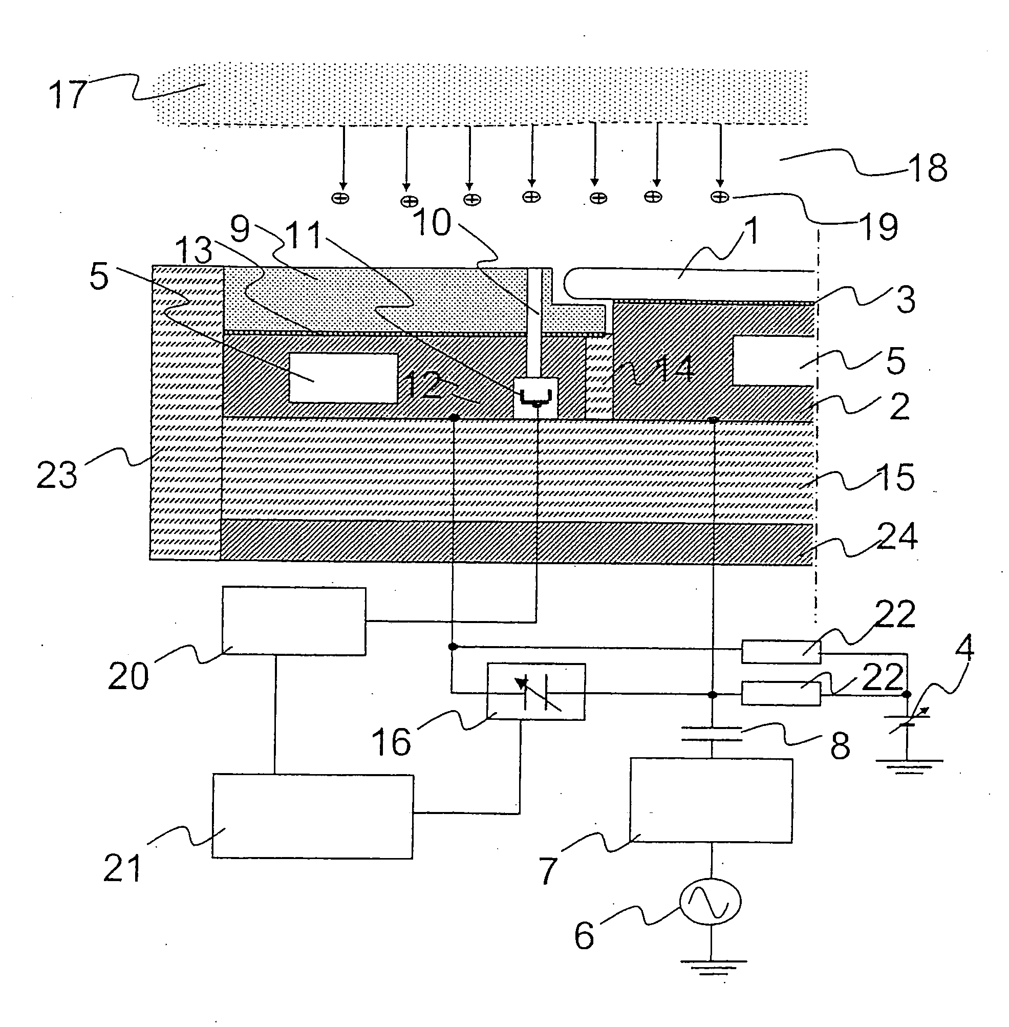
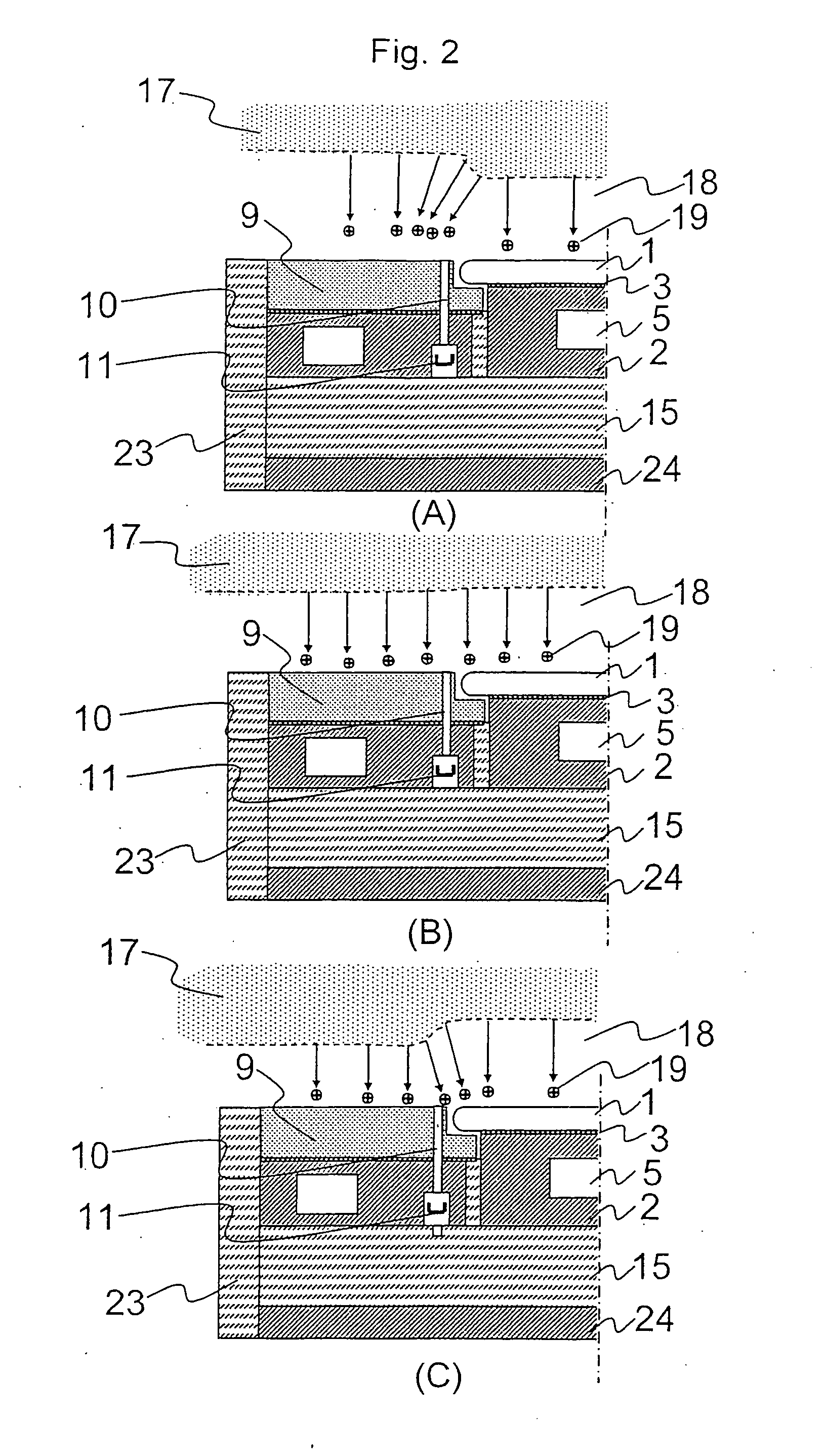
[0018]A first embodiment according to the present invention will be described with reference to FIG. 1. FIG. 1 is an enlarged view of a wafer end portion of a lower electrode 2 in a plasma processing apparatus, on which lower electrode a silicon wafer 1 as a sample to be processed is mounted. In the plasma processing apparatus according to the present invention, the silicon wafer 1 is attracted to the lower electrode 2 via an insulating film for electrostatic chuck 3. Further, the electrostatic chuck force is controlled by a DC power source 4. The lower electrode 2 is cooled by a liquid or gas refrigerant which is made to flow through a refrigerant passage 5. A high-frequency voltage for drawing ions to the wafer is supplied to the lower electrode 2 from a high-frequency power supply 6 via a matching circuit 7 and a blocking capacitor 8.

[0019]At the periphery of the silicon wafer 1, an annular conductor member, for example, a focus ring 9 made of silicon is arranged concentrically w...


PUM

PropertyMeasurementUnit
Lengthaaaaaaaaaa
Depthaaaaaaaaaa
Depthaaaaaaaaaa

Abstract

To make it possible to suppress deterioration of processing properties of a sample to be processed due to the distortion of ion sheath at the end portion of the sample to be processed or possible to maintain the condition for suppressing the deterioration, so that the acquisition rate of acceptable products can be increased, so as to thereby improve the yield. In a plasma processing apparatus, a minute hole 10 is provided in a focus ring 9 in the vicinity of the inner circumferential portion thereof. Current detecting means 11 is arranged in the bottom portion of the minute hole 10. A high-frequency power is supplied to the focus ring 9 via high-frequency power distributing means 16. A state of distortion of an ion sheath 18 is detected from an amount of current which is changed according to the amount of the high-frequency power supplied to the focus ring 9 and which is detected by current detecting means 11. Further, the amount of high-frequency power supplied to the focus ring 9 is controlled by a control section 21 so as to correct the detected distortion state.

Description

[0001]The present application is based on and claims priority of Japanese patent application No. 2008-181287 filed on Jul. 11, 2008, the entire contents of which are hereby incorporated by reference.BACKGROUND OF THE INVENTION[0002]1. Field of the Invention[0003]The present invention relates to a semiconductor manufacturing apparatus for manufacturing a semiconductor device. More particularly, the present invention relates to a plasma processing apparatus using a dry etching technique for etching, by using the plasma, semiconductor materials, such as silicon and a silicon oxide film, according to a mask pattern shape formed of a resist material, and the like.[0004]2. Description of the Related Art[0005]The dry etching is a semiconductor fine processing method in which process gases are introduced into a vacuum chamber having vacuum evacuation means, so as to be converted into plasma by electromagnetic waves, and in which the surface of a sample to be processed other than a masked po...

Claims


Application Information

Patent Timeline
IPC IPC(8): C23F1/08
CPCH01J37/32642H01J37/32935H01J37/32651
Inventor YOKOGAWA, KANETSUKOBAYASHI, HIROYUKITANDOU, TAKUMIMAEDA, KENJIIZAWA, MASARU
Owner HITACHI HIGH-TECH CORP
Why Eureka
Try Eureka