Thin film transistor substrate, electronic apparatus, and methods for fabricating the same

a thin film transistor and substrate technology, applied in the direction of electrical equipment, semiconductor/solid-state device manufacturing, semiconductor devices, etc., can solve the problems of deteriorating the uniformity of electrical characteristics of the tfts, reducing the mobility of carriers in the channel region, and prone to being trapped in the sgbs, so as to improve the uniformity of electrical properties.

Active Publication Date: 2010-01-28
AU OPTRONICS CORP
View PDF8 Cites 3 Cited by
  • Summary
  • Abstract
  • Description
  • Claims
  • Application Information

AI Technical Summary

Benefits of technology

[0012]The present invention is directed to a TFT array substrate by which uniformity of electrical properties can be improved.

Problems solved by technology

On the contrary, when the line connecting the centroid of the source region with the centroid of the drain region is parallel to the MGBs, the carriers are prone to be trapped in the SGBs, such that the carrier mobility in the channel region is reduced.
Since the carrier mobility in the channel region is closely related to the crystallization form of the polysilicon, the anisotropic property of the polysilicon leads to variations in characteristics of the TFTs on the TFT array substrate, thereby deteriorating uniformity of electrical characteristics of the TFTs.
As such, mura effects may be generated, and display quality is reduced.

Method used


Image

  • Thin film transistor substrate, electronic apparatus, and methods for fabricating the same
  • Thin film transistor substrate, electronic apparatus, and methods for fabricating the same
  • Thin film transistor substrate, electronic apparatus, and methods for fabricating the same

Examples


first embodiment

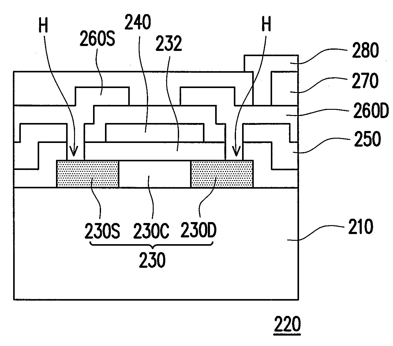
[0036]FIG. 3 illustrates a schematic top view of a TFT array substrate according to a first embodiment of the present invention and a partial enlarged view of said TFT array substrate. Referring to FIG. 3, a TFT array substrate 200 includes a substrate 210 and at least a TFT 220 disposed on the substrate 210. The TFT 220 includes a semiconductor island 230 and at least a gate 240. The semiconductor island 230 includes a source region 230S, a drain region 230D, and a channel region 230C positioned between the source region 230S and the drain region 230D. Here, the semiconductor island 230 can be made of poly-crystalline silicon, mono-crystalline silicon, or micro-crystalline silicon. In an alternative, the semiconductor island 230 can be made of a poly-crystalline compound containing silicon and at least one of germanium, arsenide, and gallium, a mono-crystalline compound containing the same, or a micro-crystalline compound containing the same. The material of the semiconductor islan...

second embodiment

[0043]FIG. 6 illustrates a schematic top view of a TFT array substrate according to a second embodiment of the present invention and a partial enlarged view of said TFT array substrate. Referring to FIG. 6, a TFT array substrate 300 includes a substrate 210 and at least a TFT 320 disposed on the substrate 210. The TFT 320 includes a semiconductor island 230 and a gate 240. The semiconductor island 230 has a plurality of SGBs. Besides, the semiconductor island 230 includes a source region 230S, a drain region 230D, and a channel region 230C positioned between the source region 230S and the drain region 230D. The gate 240 corresponds to the channel region 230C. The material of the semiconductor island 230, the material of the substrate 210, and the corresponding arrangement of the gate 240 and the channel region 230C are similar to those described in the first embodiment, and the TFT 320 herein has a top-gate structure, for example. Hence, no further descriptions are provided herein. ...


PUM


Abstract

A TFT substrate includes a substrate and at least a TFT disposed thereon. The TFT includes a semiconductor island and at least a gate. The semiconductor island has a source region, a drain region, and a channel region interposed therebetween. The semiconductor island has sub-grain boundaries. The gate corresponds to the channel region. A first included angle between an extending direction of the gate and a line connecting the centroid of the source region with the centroid of the drain region is not substantially equal to 90 degrees. A second included angle between the sub-grain boundaries in the channel region and the line connecting the centroid of the source region with the centroid of the drain region is not substantially equal to 0 degree or 90 degrees. Additionally, a method of fabricating a TFT substrate, an electronic apparatus, and a method of fabricating the electronic apparatus are also provided.

Description

CROSS-REFERENCE TO RELATED APPLICATION[0001]This application claims the priority benefit of Taiwan application serial no. 97128473, filed on Jul. 25, 2008. The entirety of the above-mentioned patent application is hereby incorporated by reference herein and made a part of this specification.BACKGROUND OF THE INVENTION[0002]1. Field of the Invention[0003]The present invention relates to a thin film transistor (TFT) substrate, an electronic apparatus, and methods for fabricating the same and, more particularly, relates to a TFT substrate in which a channel region has sub-grain boundaries and relates to an arrangement of the sub-grain boundaries, an electronic apparatus, and methods for fabricating the same.[0004]2. Description of Related Art[0005]Recently, with an advancement of optoelectronic technologies and semiconductor fabricating technologies, a flat panel displays have been vigorously developed. Among the flat panel displays, a liquid crystal displays (LCDs) characterized by lo...

Claims


Application Information

Patent Timeline
Patent Type & Authority Applications(United States)
IPC IPC(8): H01L33/00H01L21/00
CPCH01L29/66757H01L27/1296
Inventor SUN, MING-WEICHAO, CHIH-WEI
Owner AU OPTRONICS CORP
Why Eureka
Try Eureka