Electrophotographic photosensitive member and electrophotographic apparatus

a photosensitive member and electrophotography technology, applied in the direction of electrophotography process apparatus, instruments, corona discharge, etc., can solve the problems of increasing the load of the electrophotographic photosensitive member, the abrasion amount of the surface layer occasionally suddenly increasing, and the image blurring, etc., to prolong the life of the electrophotographic apparatus, superior adhesiveness and abrasion resistance, and superior durability

Inactive Publication Date: 2010-01-28
CANON KK
View PDF10 Cites 22 Cited by
  • Summary
  • Abstract
  • Description
  • Claims
  • Application Information

AI Technical Summary

Benefits of technology

[0007]An object of the present invention is to provide an electrophotographic photosensitive member which has a wide band gap to rays having short wavelengths, is provided with a surface layer superior in adhesiveness and abrasion resistance, and is thereby superior in durability. In other words, the object is to provide an electrophotographic photosensitive member which inhibits an image blur and a ghost originating in the peeling of the surface layer from the interface in the electrophotographic photosensitive member, the melt-adhesion of a toner with the electrophotographic photosensitive member and the abrasion of the surface layer, is suitable for an electrophotographic apparatus that forms a fine image at a high speed, and can extend the life of the electrophotographic apparatus. The object of the present invention is also to provide an electrophotographic photosensitive member which promotes an interaction between a photoconductive layer and the surface layer, and has enhanced light sensitivity.
[0009]The present inventors made an extensive investigation on the electrophotographic photosensitive member so as to find out a surface layer which has high transmissivity to rays having short wavelengths and is superior in adhesiveness and abrasion resistance, and as a result, accomplished the present invention.
[0013]The present invention can provide an electrophotographic photosensitive member which has a wide band gap to rays having short wavelengths, has a surface layer superior in adhesiveness and abrasion resistance, and thereby is superior in durability. In other words, the present invention can provide an electrophotographic photosensitive member which inhibits an image blur and a ghost originating in the peeling of the surface layer from the interface in the electrophotographic photosensitive member, the melt-adhesion of a toner with the electrophotographic photosensitive member and the abrasion of the surface layer, is suitable for an electrophotographic apparatus that forms a fine image at a high speed, and can extend the life of the electrophotographic apparatus. The present invention can also provide an electrophotographic photosensitive member which promotes an interaction between a photoconductive layer and the surface layer, and has enhanced light sensitivity.

Problems solved by technology

Furthermore, when the processing speed of forming an image is increased according to the request of increasing a printing speed of the electrophotographic apparatus, the load for the electrophotographic photosensitive member increases, so that when the image is repeatedly formed with the use of a conventional electrophotographic photosensitive member at a high speed for a long period of time, various problems arise.
Specifically, a part of the surface layer is lifted up from a photoconductive layer in a fine region with a diameter of approximately several micrometers, and as a result, the outline of the image occasionally spreads and becomes unclear to cause image blurring, or the abrasion amount of the surface layer occasionally suddenly increases during use.
From that point of view, the electrophotographic photosensitive member having the surface layer formed from the above described aluminum oxide material containing zinc is difficult to be applied to an electrophotographic apparatus which forms the image at the high speed.

Method used


Image

  • Electrophotographic photosensitive member and electrophotographic apparatus
  • Electrophotographic photosensitive member and electrophotographic apparatus
  • Electrophotographic photosensitive member and electrophotographic apparatus

Examples


example 7 to 14

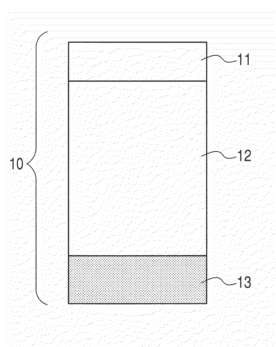
[0132]Electrophotographic photosensitive members (samples 13 to 19) were produced by using a cylinder which was made from aluminum, had the outer diameter of 84 mm, the length of 381 mm and the wall thickness of 3 mm, and had the surface mirror-finished, as a conductive substrate, and by forming a lower electric-charge injection preventing layer, a photoconductive layer, an intermediate layer and a surface layer thereon. The samples 13 to 19 (Examples 7 to 13) were produced by adopting an a-SiN layer as the intermediate layer in which the content of a nitrogen atom with respect to a silicon atom in the intermediate layer was changed by adjusting the flow rate of N2, and a sample 20 (Example 14) was produced for comparison, which had not the intermediate layer formed therein. The lower electric-charge injection preventing layer, the photoconductive layer and the intermediate layer were formed with the use of the plasma CVD apparatus illustrated in FIG. 4 in conditions shown in Table ...

examples 15 to 21

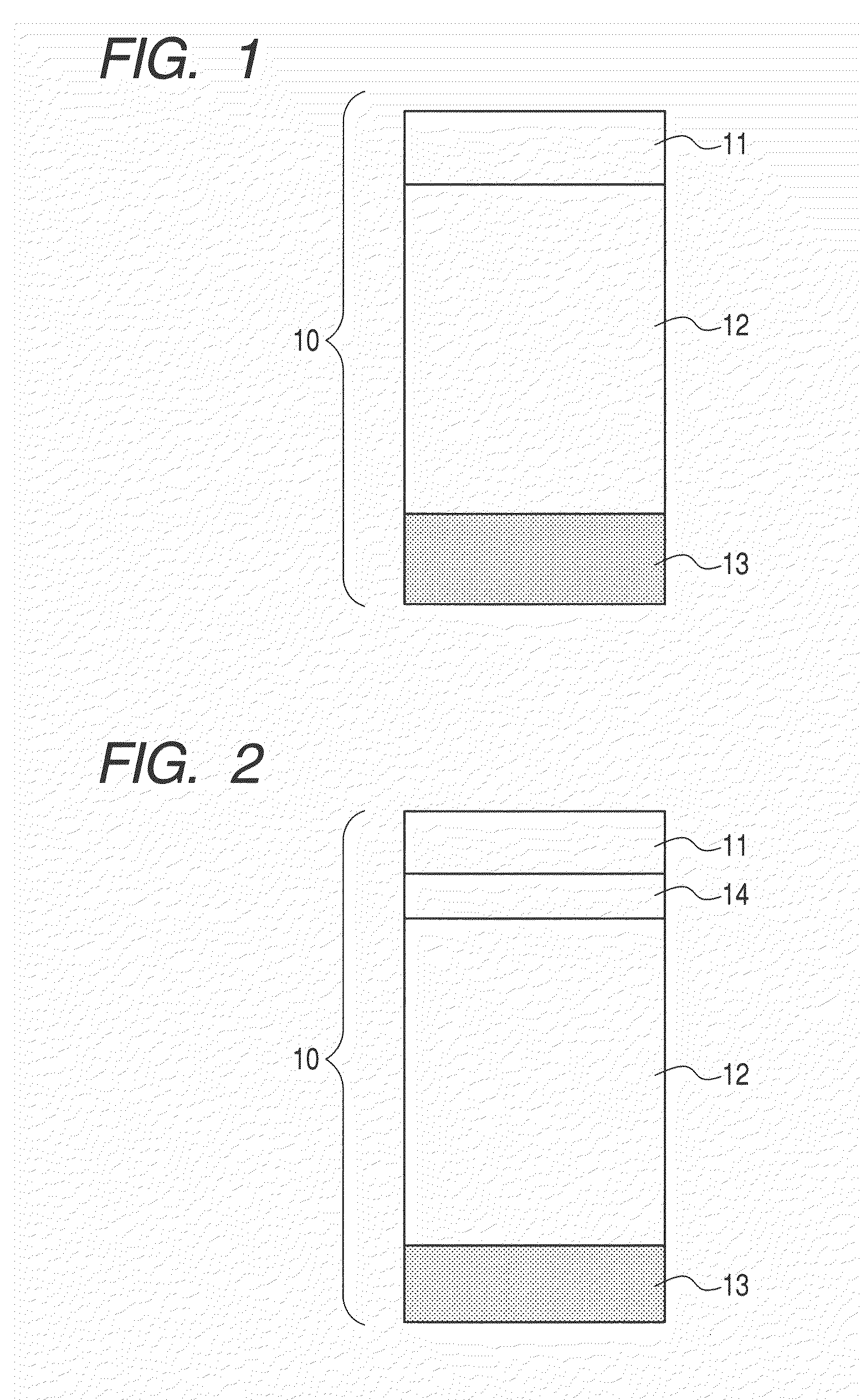
[0137]Electrophotographic photosensitive members (samples 21 to 27) were formed by forming a lower electric-charge injection preventing layer and a photoconductive layer in conditions shown in Table 11; by forming an intermediate layer in conditions shown in Table 11 through adopting an a-SiC layer as the intermediate layer and changing the content of a carbon atom with respect to a silicon atom in the intermediate layer by adjusting the flow rate of CH4 as shown in Table 12; and by forming other parts in a similar method to that in Example 7.

TABLE 11Lower electric-chargeinjectionpreventingPhotoconductiveIntermediatelayerlayerlayerFlow rate of gasSiH4 [ml / min20020050(normal)]H2 [ml / min (normal)]850650100B2H6 (ppm)10001.5(with respect to SiH4)NO [ml / min (normal)]10CH4 [ml / min (normal)]Table 12Pressure [Pa]807560High-frequency200800600power [w]Substrate temperature250270240[° C.]Film thickness [μm]3300.1

TABLE 12SampleSampleSampleSampleSampleSample212223Sample 24252627Flow rate of CH41...

examples 22 to 24

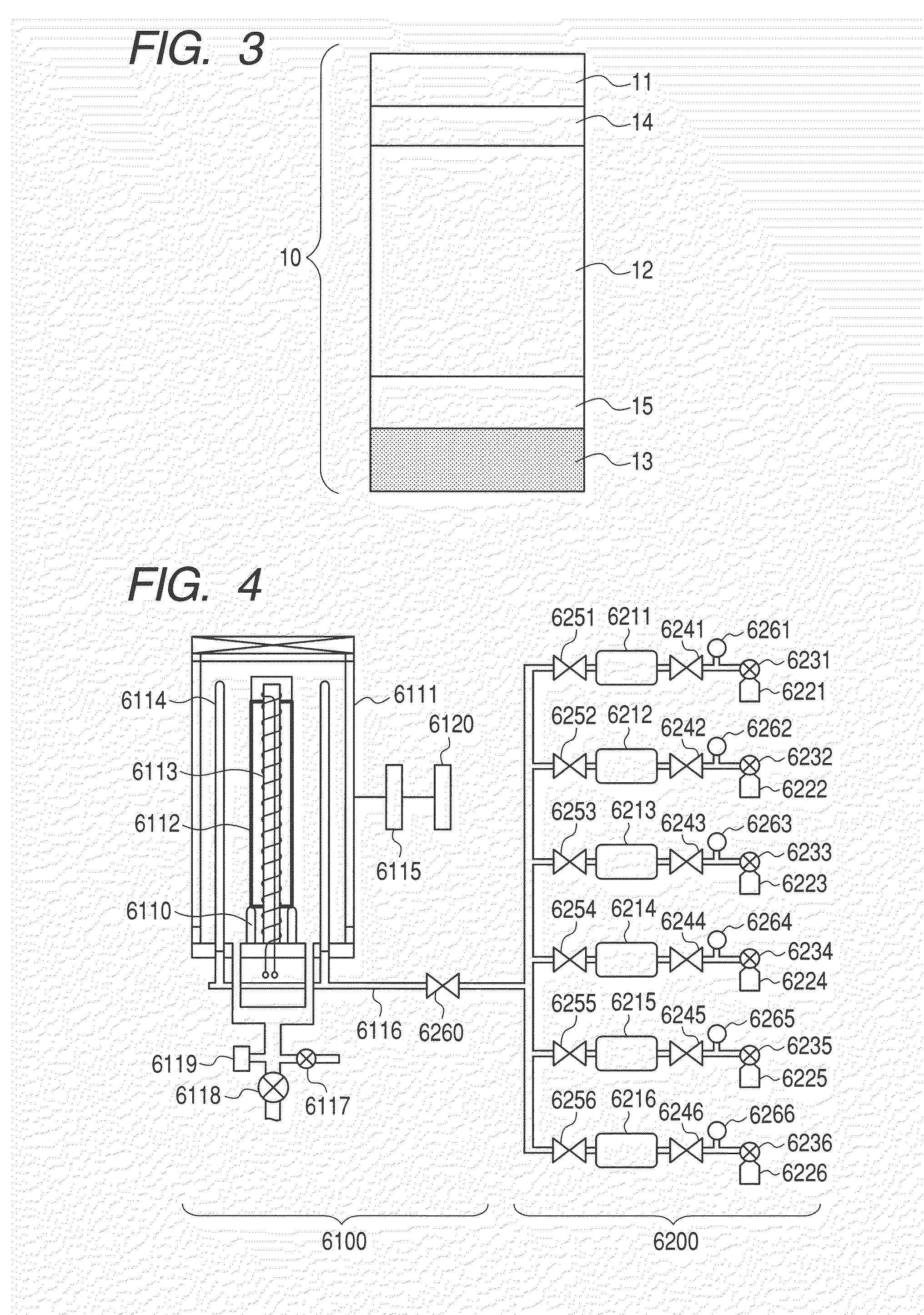
[0142]Electrophotographic photosensitive members (samples 28 to 30) were produced by forming a lower electric-charge injection preventing layer and a photoconductive layer in conditions shown in Table 14; by forming an intermediate layer in conditions shown in Table 15 through using magnesium fluoride (MgF2), magnesium oxide (MgO) and lanthanum fluoride (LaO3) respectively with the use of a sputtering apparatus illustrated in FIG. 5; and by forming other parts in a similar method to that in Example 7.

TABLE 14Lowerelectric-chargeinjectionPhotoconductivepreventing layerlayersFlow rate of gasSiH4 [ml / min (normal)]200200H2 [ml / min (normal)]650650B2H6 (ppm) (with respect to SiH4)10001.5NO [ml / min (normal)]10Pressure [Pa]8075High-frequency power [w]200800Substrate temperature [° C.]270270Film thickness [μm]330

TABLE 15Intermediate layerSample 28Sample 29Sample 30TargetMgF2MgOLaF3Flow rate of gasAr [ml / min (normal)]757575F2 [ml / min (normal)]2.02.3O2 [ml / min (normal)]1.5Pressure [Pa]0.30.30....


PUM


Abstract

The present invention provides an electrophotographic photosensitive member in which a photoconductive layer is an amorphous layer that contains a silicon atom as a main component, and a surface layer contains an aluminum atom, a zinc atom and an oxygen atom so as to satisfy Expression (1) and Expression (2):3.0≦100 {y / (x+y)}≦7.0   (1), and1.05≦z / (1.50x+y)≦1.20   (2),in Expression (1) and Expression (2), x represents atom % of the aluminum atom contained in the surface layer, y represents atom % of the zinc atom contained in the surface layer, and z represents atom % of the oxygen atom contained in the surface layer.

Description

BACKGROUND OF THE INVENTION[0001]1. Field of the Invention[0002]The present invention relates to an electrophotographic photosensitive member and an electrophotographic apparatus having the electrophotographic photosensitive member.[0003]2. Description of the Related Art[0004]An amorphous deposited film (amorphous-silicon-deposited film) which contains a silicon atom as a main component and further contains a hydrogen atom, a halogen atom and the like has high performance and high durability and causes no pollution when used as a photosensitive member of an electrophotographic photosensitive member to be used in an electrophotographic apparatus, and is commercially used. Electrophotographic photosensitive members having various layer structures with the use of such a deposited film are proposed so as to meet various requirements for the performance. Among them, the electrophotographic photosensitive member provided with a surface layer has superior abrasion resistance, charge retent...

Claims


Application Information

Patent Timeline
Patent Type & Authority Applications(United States)
IPC IPC(8): G03G15/00
CPCG03G5/08228G03G15/751G03G5/08242
Inventor AKIYAMA, KAZUYOSHIOZAWA, TOMOHITONISHIMURA, YUU
Owner CANON KK
Why Eureka
Try Eureka