

Transistor device and method of manufacturing such a transistor device
a transistor and transistor technology, applied in the field of transistor devices, can solve the problems of unsuitable conventional systems for high-scale integration with simultaneous proper performance, and achieve the effect of high device performance and suitability for high-scale integration
- Summary
- Abstract
- Description
- Claims
- Application Information
AI Technical Summary
Benefits of technology
Problems solved by technology
Method used
Image

Examples
Embodiment Construction
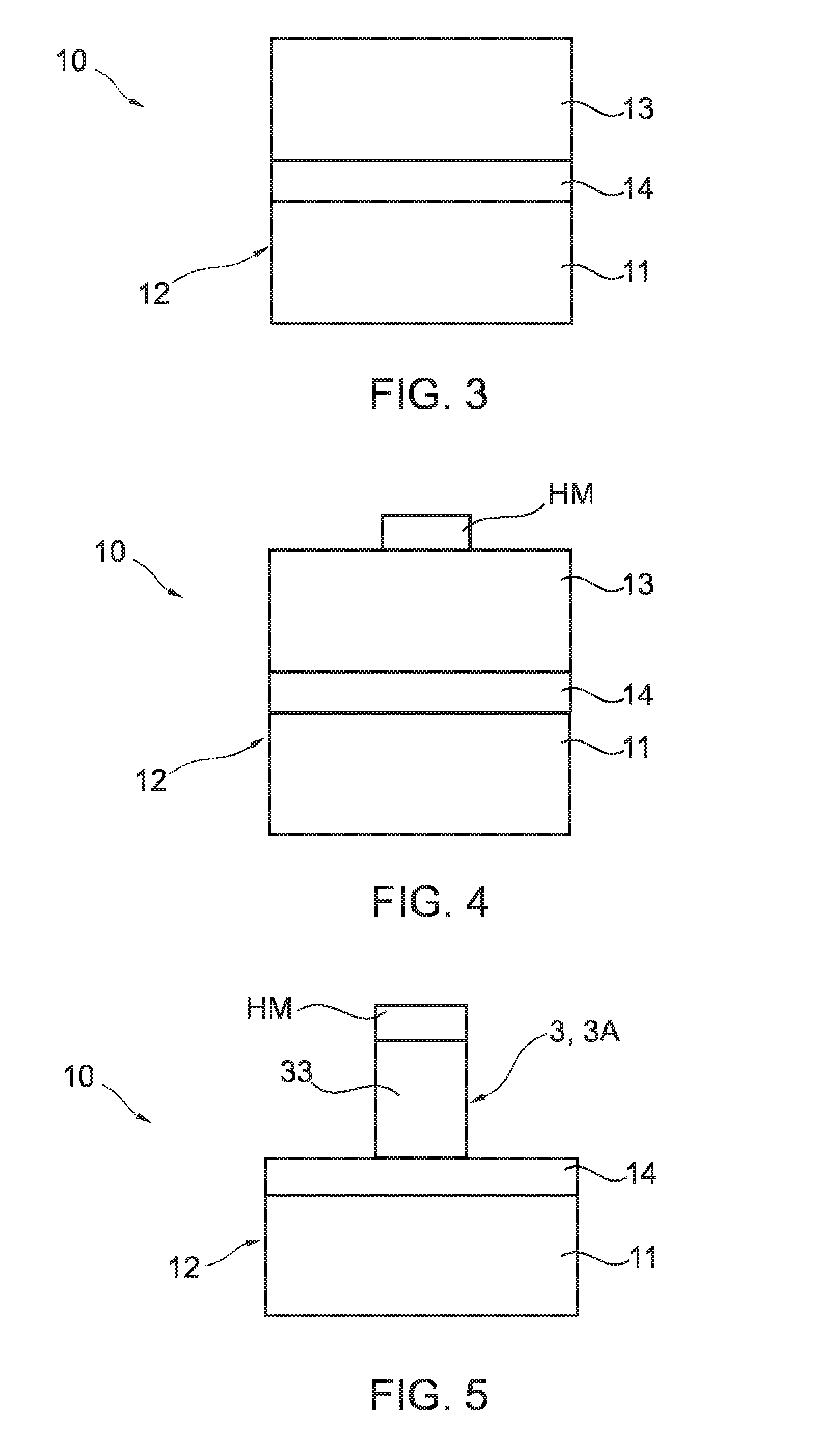
[0066]The figures are diagrammatic and not drawn to scale, the dimensions in the thickness direction being particularly exaggerated for greater clarity. Corresponding parts are generally given the same reference numerals and the same hatching in the various figures.
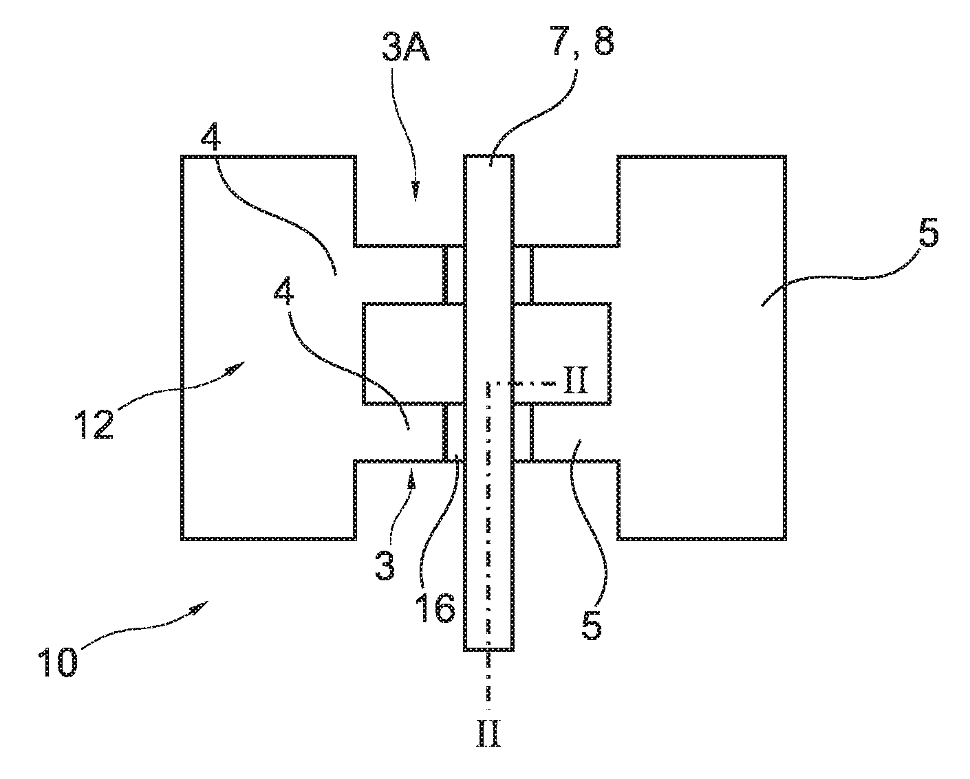
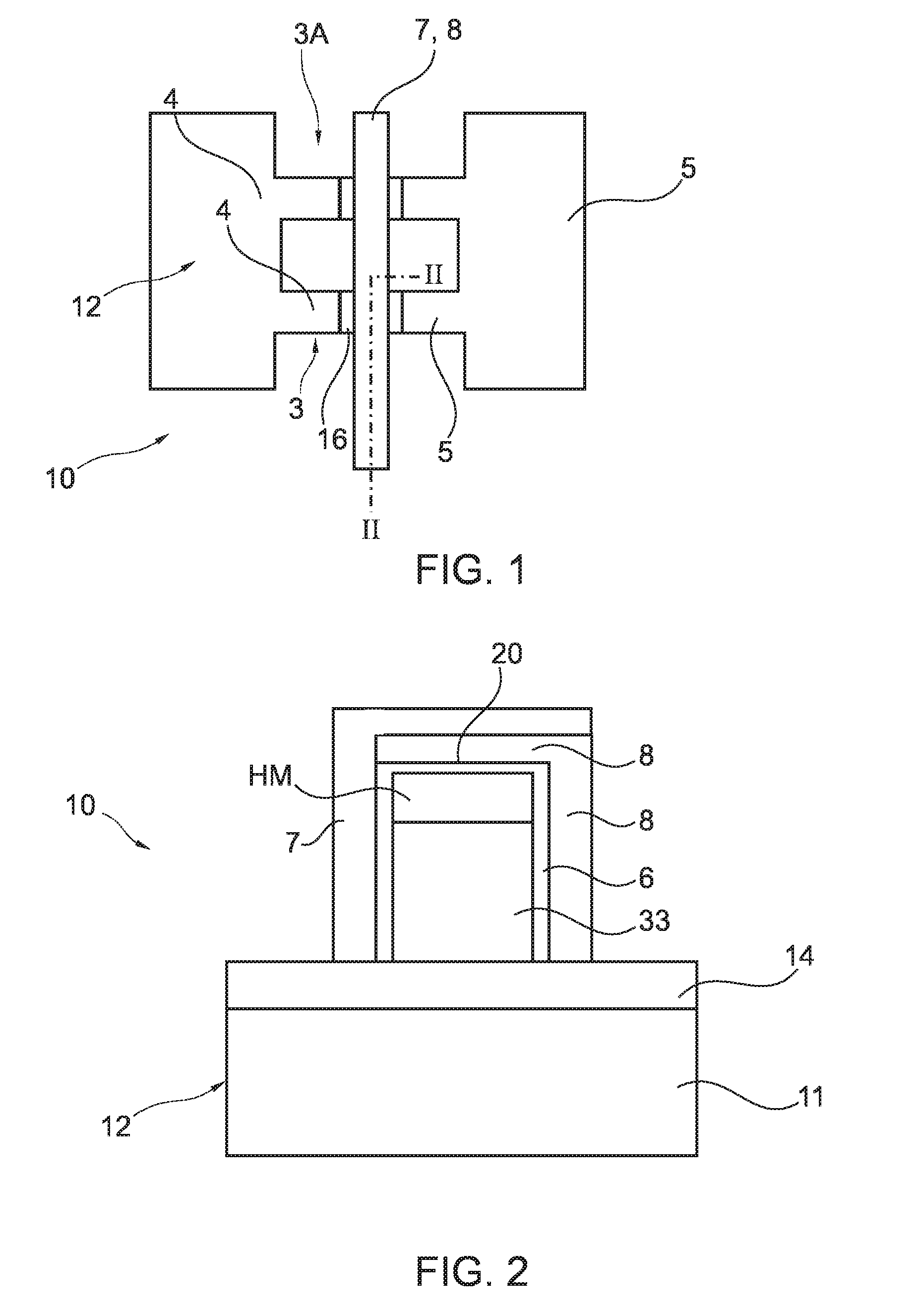
[0067]FIG. 1 shows a top view of an embodiment of a semiconductor sensor device according to an exemplary embodiment of the invention and FIG. 2 shows a cross-section perpendicular to the thickness direction and along the line II-II of the semiconductor sensor device of FIG. 1. The device 10 of this example comprises a substrate 11, in this case of intrinsic silicon which is coated with an electrically insulating layer 14 of silicon dioxide on top of which a silicon region 33 is present forming a part of the semiconductor body 12. The latter comprises a source region 4 (which may also be denoted as a first source / drain region), here of the P-type conductivity and a drain region 5 (which may also be denoted as a second sou...
PUM
 Abstract
Description
Claims
Application Information