Lithography for pitch reduction

Inactive Publication Date: 2010-02-04
NXP USA INC +1
View PDF12 Cites 18 Cited by
  • Summary
  • Abstract
  • Description
  • Claims
  • Application Information

AI Technical Summary

Benefits of technology

[0049]In another embodiment, the subl

Problems solved by technology

While developments are under way to provide high numerical aperture exposure systems and/or increase the coefficient P to minimum feature size F, the rate of reduction of the minimum feature size F through such efforts is far slower than the rate of reduction of desired feature sizes for high performance of semiconductor devices.
Further, obtaining light sources that provide reduced wavele

Method used


Image

  • Lithography for pitch reduction
  • Lithography for pitch reduction
  • Lithography for pitch reduction

Examples


first embodiment

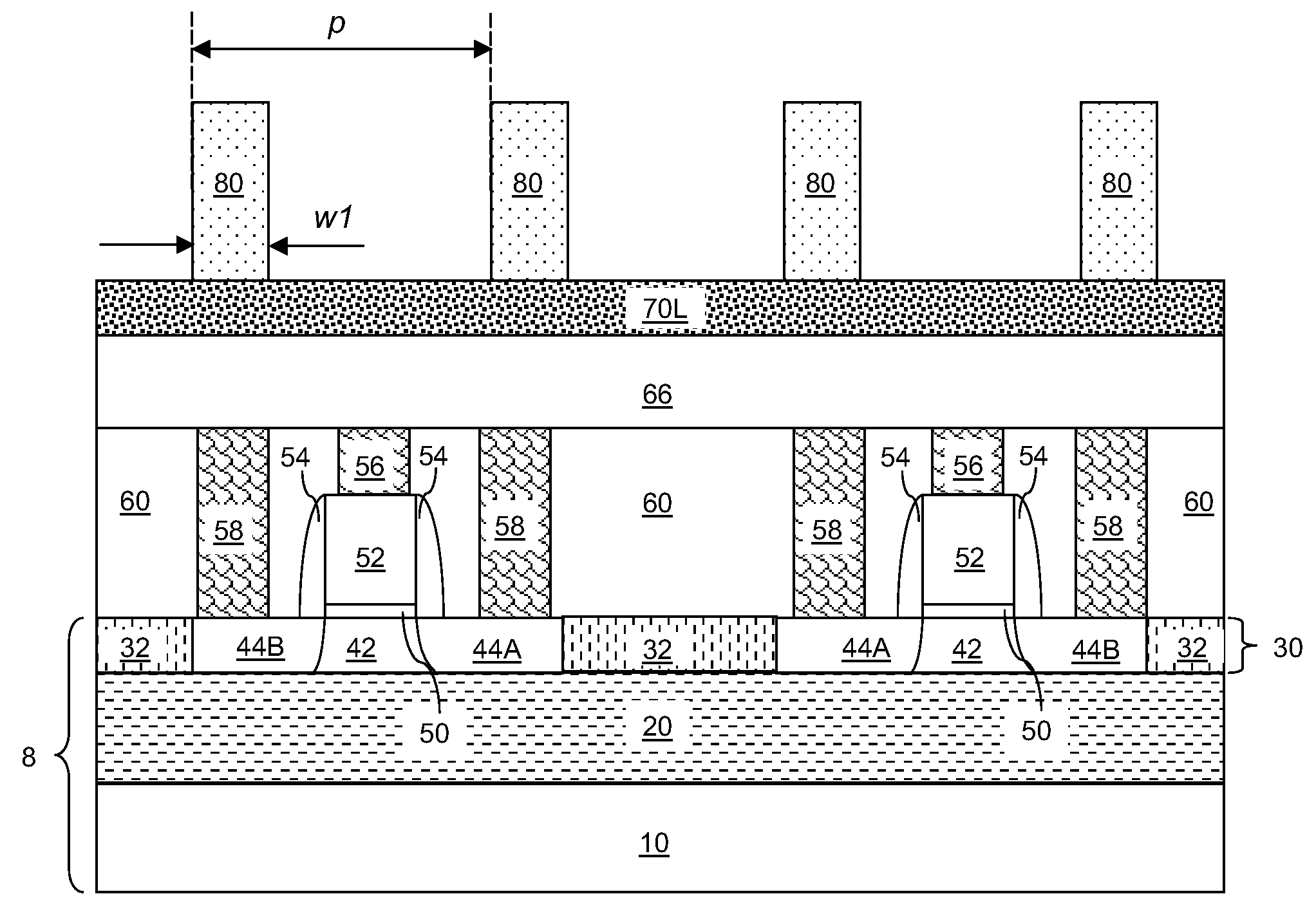
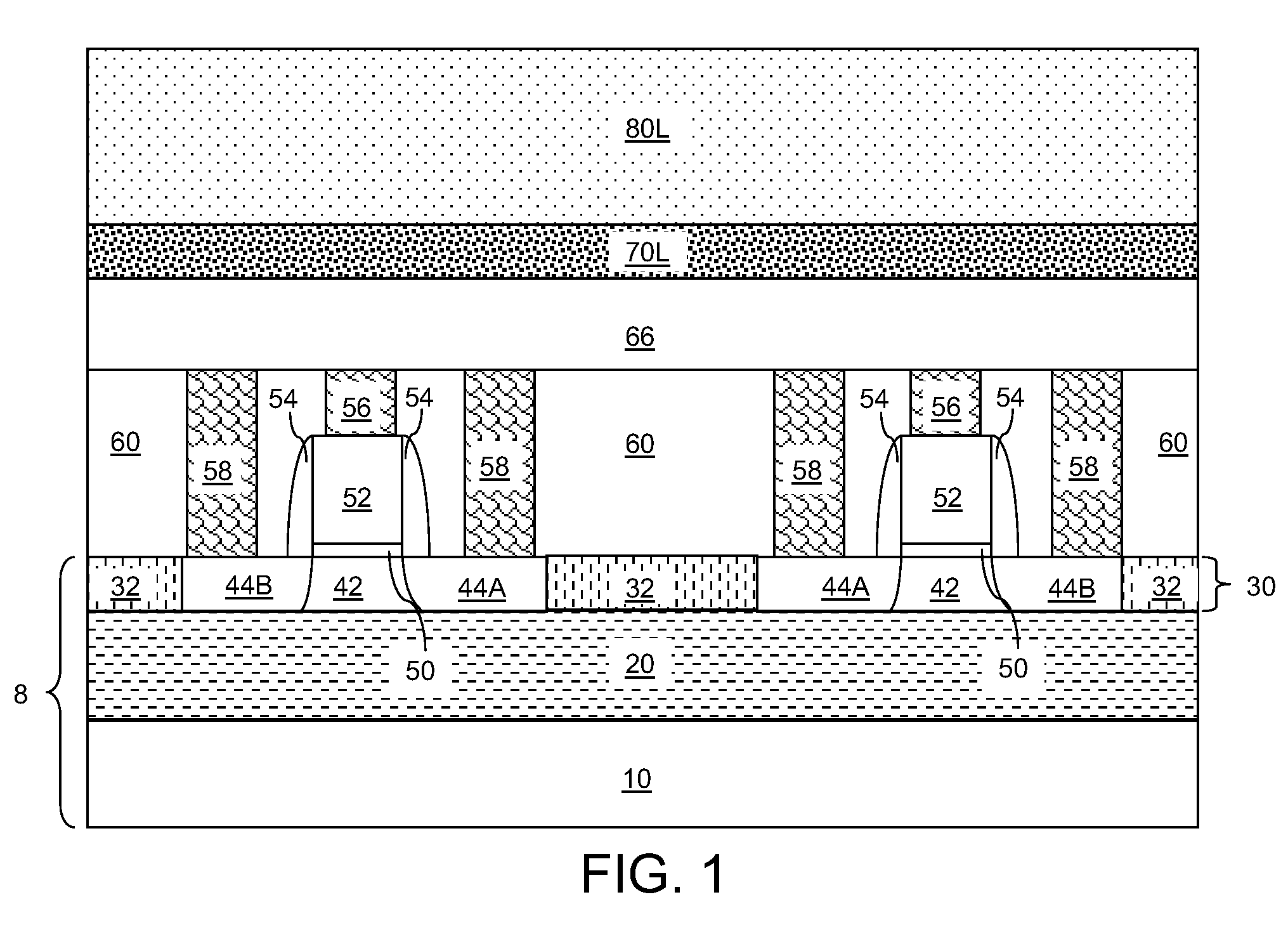
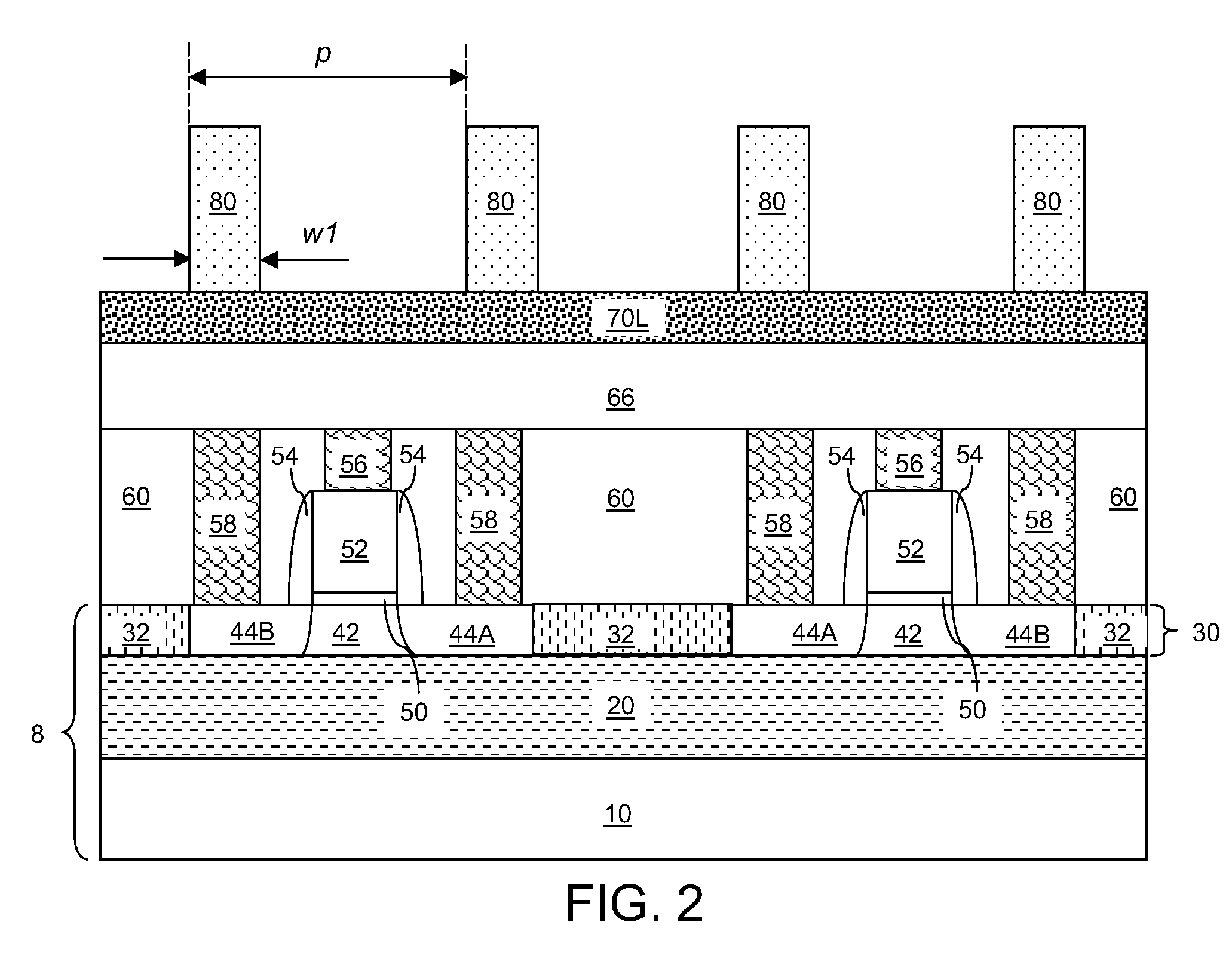
[0067]Referring to FIG. 1, a first exemplary lithographic structure according to the present invention comprises a semiconductor structure including a semiconductor substrate 8, semiconductor device structures, an underlying layer 66, an optically dense layer 70L, and a photoresist layer 80. The semiconductor substrate 8 and the semiconductor device structure beneath the underlying layer 66 are shown only for the purposes of illustration. In general, the present invention may be employed on any substrate on which, or in which, an underlying layer is formed.

[0068]The semiconductor substrate 8 may be a semiconductor-on-insulator (SOI) substrate, which comprises a handle substrate 10, a buried insulator layer 20, and a top semiconductor layer 30. Alternately, the semiconductor substrate 8 may be a bulk substrate or a hybrid substrate having a bulk portion and a semiconductor-on-insulator portion. Semiconductor devices, which may be field effect transistors or any other semiconductor de...

second embodiment

[0091]Referring to FIG. 8, a second exemplary lithographic structure according to the present invention comprises a semiconductor structure including a semiconductor substrate 8, semiconductor device structures, an underlying layer 66, a first optically dense layer 170L, and a first anti-reflective coating (ARC) layer 180L, and a first photoresist layer 180L. The semiconductor substrate 8 and the semiconductor device structure beneath the underlying layer 66 are shown only for the purposes of illustration. In general, the present invention may be employed on any substrate on which, or in which, an underlying layer is formed.

[0092]The semiconductor substrate 8 and the semiconductor device structures may be any such structures known in the art, and may be the same as in the first exemplary lithographic structure. The underlying layer 66 may comprise a dielectric layer, a semiconductor layer, a conductive layer, or a stack thereof. In general, the underlying layer 66 may comprise any m...


PUM


Abstract

In one embodiment, a photoresist is lithographically patterned to form an array of patterned photoresist portions having a pitch near twice a minimum feature size. Fluorine-containing polymer spacers are formed on sidewalls of the patterned photoresist portions. The pattern of the fluorine-containing polymer spacers is transferred into an underlying layer to form a pattern having a sublithographic pitch. In another embodiment, a first pattern in a first photoresist is transferred into a first ARC layer underneath to form first ARC portions. A planarizing second optically dense layer, a second ARC layer, and a second photoresist are applied over the first ARC portions. A second pattern in the second photoresist is transferred into the second ARC layer to form second ARC portions. The combination of the first ARC portions and second ARC portions function as an etch mask to pattern an underlying layer with a composite pattern having a sublithographic pitch.

Description

FIELD OF THE INVENTION [0001]The present invention relates to semiconductor processing methods, and particularly to methods for forming reduced pitch lithographic structures, and structures for effecting the same.BACKGROUND OF THE INVENTION [0002]Lithography is employed in semiconductor manufacturing to pattern features in a photoresist. A layer of photoresist is exposed to incident light, which may be deep-ultraviolet (DUV) radiation, mid-ultraviolet (MUV) radiation, or X-ray radiation. Alternately, the layer of photoresist may be exposed to energetic electron in e-beam lithography. The energy of the photons or electrons causes changes in chemical composition of exposed portions of the photoresist, for example, by cross-linkage, scission, side chain removal, etc. Pre-baking or post-baking of the photoresist may be employed to maximize the changes in the chemical properties of the exposed portion of the photoresist relative to unexposed portions of the photoresist.[0003]The exposed ...

Claims


Application Information

Patent Timeline
IPC IPC(8): G03F7/20
CPCH01L21/0338H01L21/0337
Inventor HOLMES, STEVEN J.HUA, XUEFENGCONLEY, WILLARD E.
Owner NXP USA INC
Why Eureka
Try Eureka