Semiconductor device and method of manufacturing the same

Inactive Publication Date: 2010-02-11
SONY CORP
View PDF2 Cites 57 Cited by
  • Summary
  • Abstract
  • Description
  • Claims
  • Application Information

AI Technical Summary

Benefits of technology

[0032]According to the present invention, a semiconductor device can be fabricated by the simple process in which both a device portion and a terminal portion surrounding the device portion are formed to have a super junction structure.
[0033]In addition, according to the first embodiment of the invention, the overlap of the lateral RESUR

Problems solved by technology

However, the third fabrication method has problems as to the conditions for not producing defects at the time of epitaxial growth into the trenches and as to control of the amount of the doping impurity (dopant) introduced

Method used


Image

  • Semiconductor device and method of manufacturing the same
  • Semiconductor device and method of manufacturing the same
  • Semiconductor device and method of manufacturing the same

Examples


first embodiment

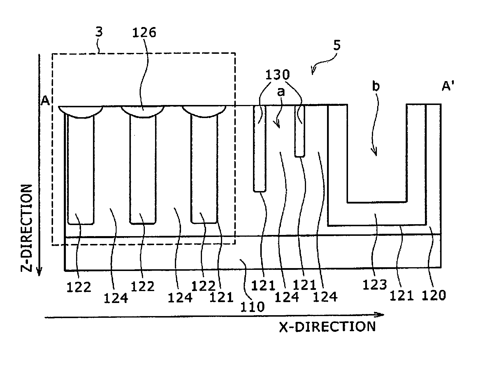
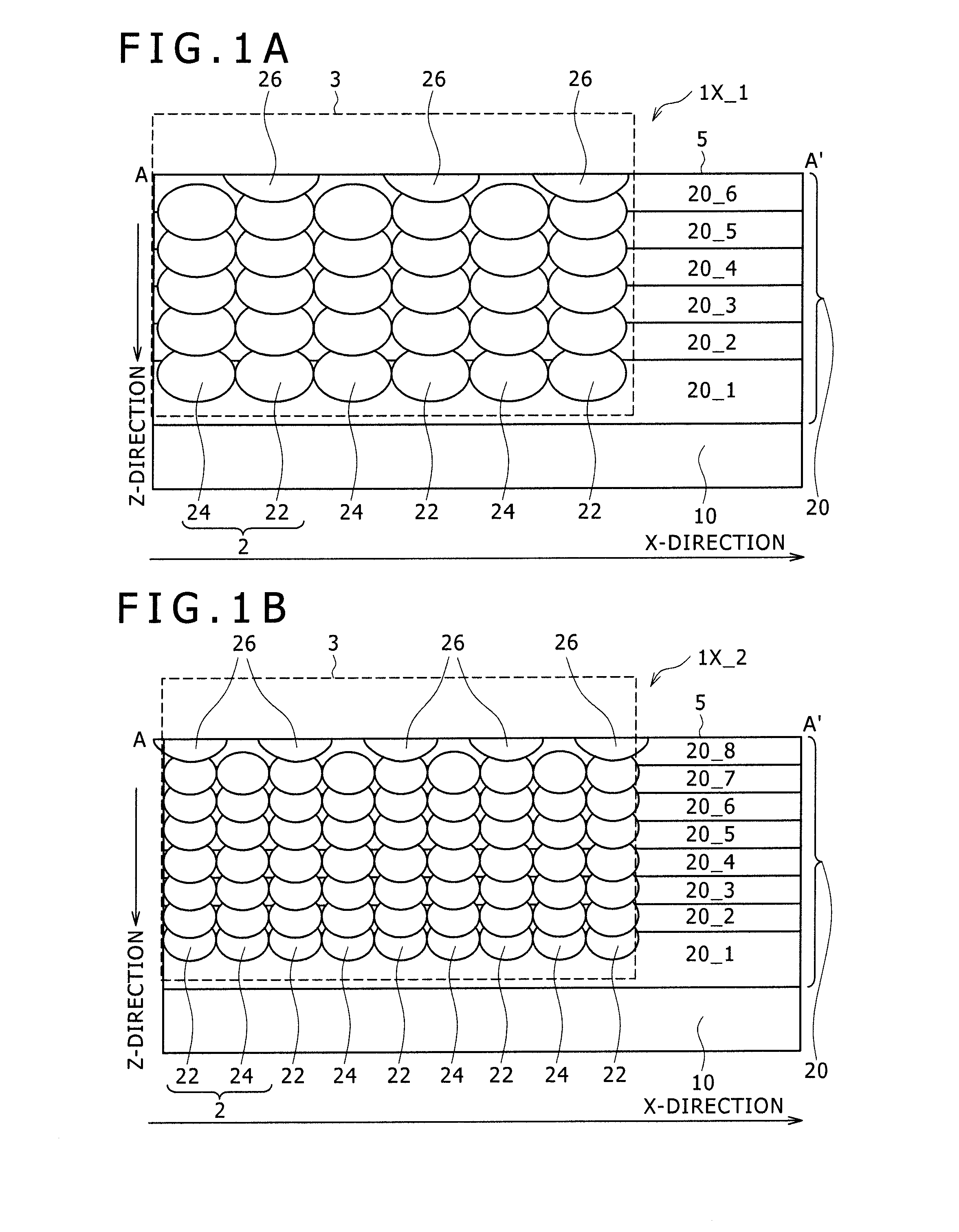
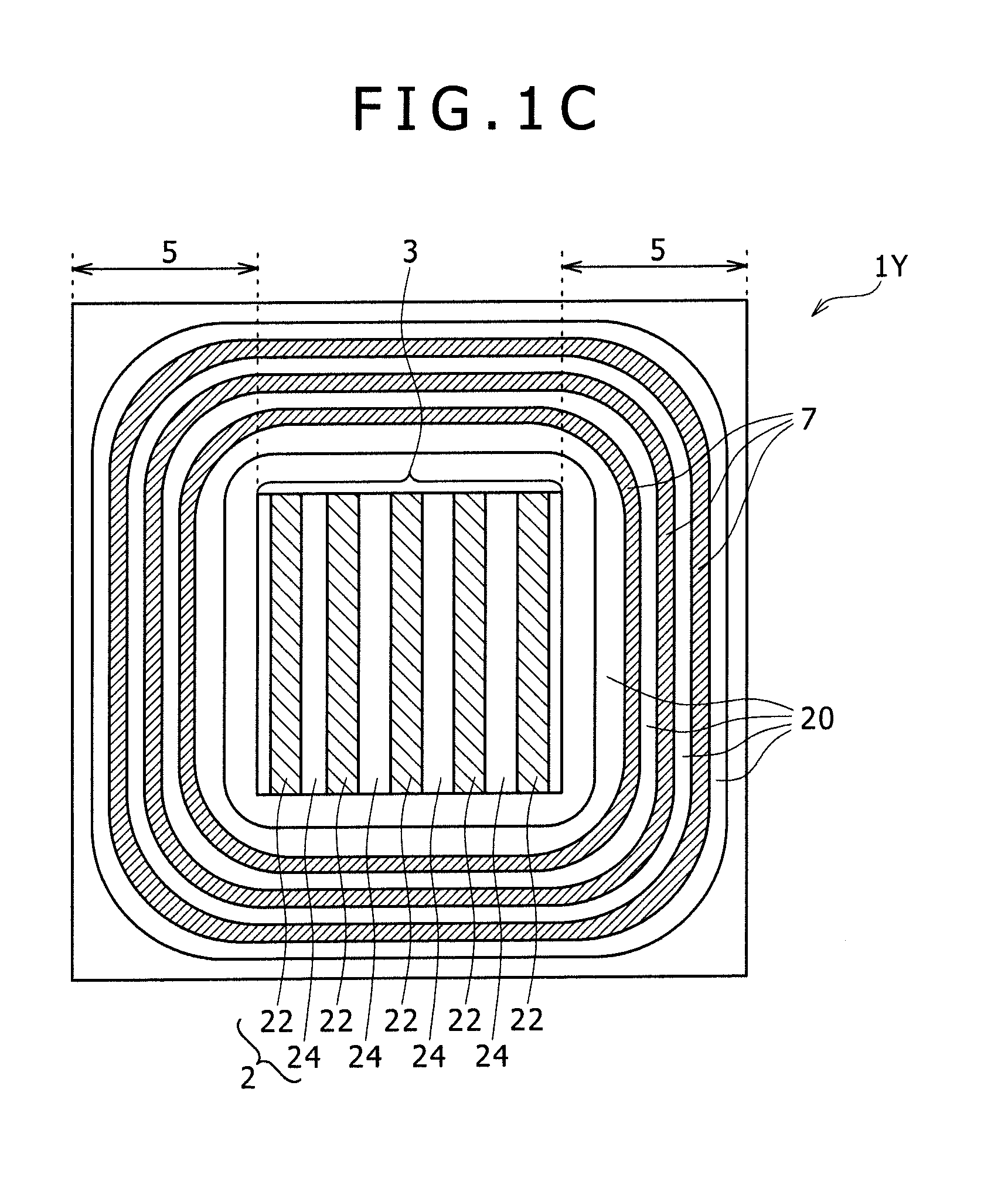
[0072]FIGS. 2A to 2E illustrate a semiconductor device 1A according to a first embodiment of the present invention. Here, FIGS. 2A and 2B show schematically the configuration of the semiconductor device 1A, wherein FIG. 2A is an XY plan view of the semiconductor device 1A, and FIG. 2B is an XZ sectional view taken along line A-A′ of FIG. 2A. Each of these figures is a schematic view and the dimensions in the drawing are not limitative, the same applying also to figures in the other embodiments. FIGS. 2C and 2D illustrate a bad influence produced in the case where a lateral RESURF structure is applied to a super junction structure. FIG. 2E illustrate bad influences produced when the trench width and the crystal plane orientation of a super junction are changed in the case of applying the third fabrication method.

[0073]The semiconductor device 1A in the first embodiment has, at a surface of an n-type high-concentration substrate 110 (n+ type drain layer) serving as an example of a fir...

second embodiment

[0105]FIGS. 3A to 3F illustrate a semiconductor device 1B according to a second embodiment of the present invention. Here, FIGS. 3A to 3D show schematically the configuration of the semiconductor device 1B of the second embodiment. FIGS. 3A and 3C are XY plan views of the semiconductor device 1B, whereas FIGS. 3B and 3D are XZ sectional views taken along line A-A′ of FIGS. 3A and 3C, respectively. FIGS. 3E and 3F illustrate a bad influence produced in the case where a lateral RESURF structure is applied to a super junction structure in the second embodiment.

[0106]The semiconductor device 1B in the second embodiment is a device in which the mechanism (setup) of the first embodiment is basically applied, and some modifications are made in the p-type epitaxial fill-up layers 123 in the terminal portion 5. The basic thought of the modifications is that of the p-type epitaxial fill-up layers 123 in the terminal portion 5, each of the portions extending from the device portion 3 in the lo...

third embodiment

[0112]FIGS. 4A to 4D illustrate a semiconductor device 1C according to a third embodiment of the present invention, showing schematically the configuration of the semiconductor device 1C of the third embodiment. FIGS. 4A and 4C are XY plan views of the semiconductor device 1C, and FIGS. 4B and 4D are XZ sectional views taken along line A-A′ of FIGS. 4A and 4C, respectively.

[0113]The semiconductor device 1C according to the third embodiment is a device in which the mechanism (setup) of the first embodiment is basically applied to the structure of the p-type epitaxial fill-up layers 123, while some modifications are applied to the p-type lateral RESURF regions 130 in the terminal portion 5. The basic thought of the modifications is characterized by a second mechanism (setup) in which, in forming the p-type lateral RESURF regions 130, the p-type lateral RESURF regions 130 are arranged in the terminal portion 5, while an apertures 132 is formed at the p-type lateral RESURF regions 130 a...


PUM


Abstract

A semiconductor device includes: a first semiconductor region of a first conductivity type disposed on the side of a first electrode; and a second semiconductor region having first pillar regions of the first conductivity type and second pillar regions of a second conductivity type, the first pillar regions and the second pillar regions being provided in paired state and alternately, in a device portion and a terminal portion surrounding the device portion, along a surface on the side of a second electrode disposed on the opposite side of the first semiconductor region from the first electrode. The semiconductor device further includes a lateral RESURF (reduced surface field) region of the second conductivity type disposed at a surface portion, on the opposite side from the first semiconductor region, of the second semiconductor region in the terminal portion.

Description

BACKGROUND OF THE INVENTION[0001]1. Field of the Invention[0002]The present invention relates to a semiconductor device and a method of manufacturing the same. More particularly, the invention relates to a semiconductor device having a super junction structure and a method of manufacturing the same.[0003]2. Description of the Related Art[0004]In recent years, there has been an increasing demand for reductions in thickness and weight of electronic apparatuses represented by liquid crystal televisions, plasma televisions, organic electroluminescence (EL) televisions, and the like. Attendant on the demand, the request for power supply apparatuses having a reduced size and an enhanced performance has also been becoming stronger. In response to the request, concern about power semiconductor devices has come to be focused on realization of improved performance, such as higher withstand voltage, larger current, lower loss, higher operating speed, and higher breakdown voltage. For example, ...

Claims


Application Information

Patent Timeline
IPC IPC(8): H01L29/66H01L21/20H01L21/768
CPCH01L29/0615H01L29/063H01L29/0634H01L29/7811H01L29/1095H01L29/66712H01L29/0696H01L21/18
Inventor HOZUMI, HIROKISASAKI, YUJISHUSAKU, YANAGAWA
Owner SONY CORP
Why Eureka
Try Eureka