Method of forming an alignment layer, and apparatus for forming the alignment layer
a technology of alignment layer and alignment layer, which is applied in the direction of photomechanical equipment, instruments, originals for photomechanical treatment, etc., can solve the problems of reducing the optical transmissivity of the pixel, narrow viewing angle of the lcd apparatus, and reducing the manufacturing yield, so as to achieve the effect of improving productivity
- Summary
- Abstract
- Description
- Claims
- Application Information
AI Technical Summary
Benefits of technology
Problems solved by technology
Method used
Image
Examples
example embodiment 1
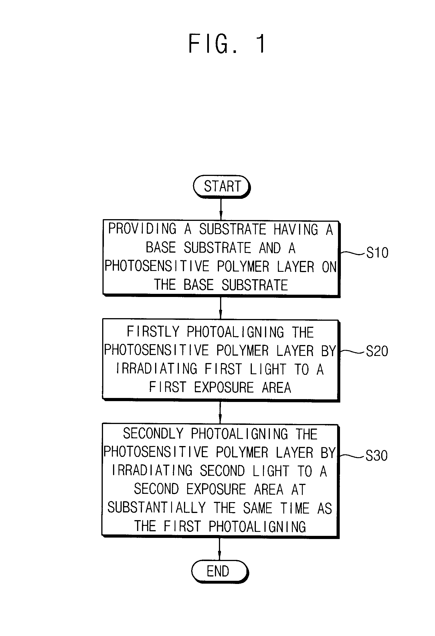
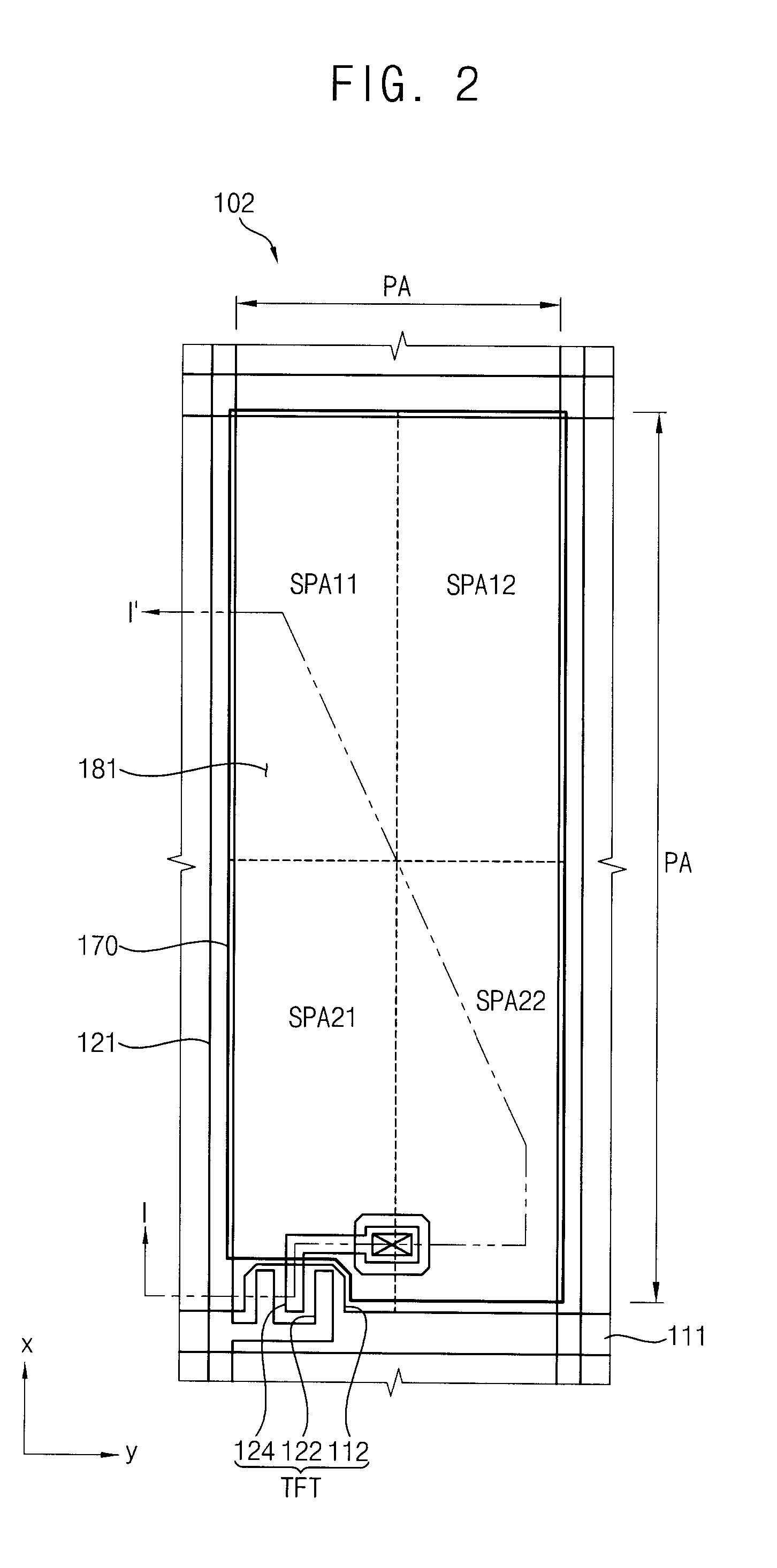
[0050]FIG. 1 is a flowchart of an exemplary embodiment of a method of forming an alignment layer in accordance with Example Embodiment 1 of the present invention. FIG. 2 is a top plan layout view illustrating a unit pixel area of a substrate formed by the method described with reference to FIG. 1.
[0051]Referring to FIG. 1, according to an exemplary embodiment of the method of forming an alignment layer in accordance with Example Embodiment 1, a substrate 102 is prepared (step S10). The substrate 102 may be a substrate which is substantially completed except for a photoalignment process for forming an alignment layer. Hereinafter, the substrate 102 is referred to as “lower substrate.”
[0052]In one exemplary embodiment, the lower substrate 102 may be a thin film transistor (“TFT”) substrate wherein pixels are driven by an active matrix driving method using a switching element. In one exemplary embodiment, the lower substrate 102 may have a substantially rectangular shape. In the exempl...
example embodiment 2
[0103]FIG. 13 is a schematic diagram illustrating an exemplary embodiment of an apparatus for forming an alignment layer in accordance with Example Embodiment 2.
[0104]An exemplary embodiment of a method of forming an alignment layer and an exemplary embodiment of a method of manufacturing an exemplary embodiment of an LCD apparatus using the method are substantially the same as those shown in FIGS. 1 to 12. Therefore, repeated and detailed descriptions will be omitted.
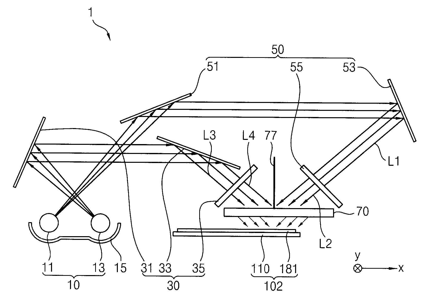
[0105]An exemplary embodiment of an apparatus 800 for forming an alignment layer described with reference to FIG. 13 may be substantially similar to the exemplary embodiment of an apparatus 1 described with reference to FIGS. 1 to 7 except that a mask 870 is divided into two mask parts which may be separately controlled. Therefore, the same reference numbers are used for the same or similar elements, and any further descriptions concerning the same or similar elements as those shown in FIGS. 1 to 7 will be omitted.
[010...
example embodiment 3
[0108]FIG. 14 is a schematic diagram illustrating another exemplary embodiment of an apparatus for forming an alignment layer in accordance with Example Embodiment 3.
[0109]An exemplary embodiment of a method of forming an alignment layer and an exemplary embodiment of a method of manufacturing an exemplary embodiment of an LCD apparatus using the exemplary embodiment of a method are substantially the same as those shown in FIGS. 1 to 12. Therefore, repeated and detailed descriptions will be omitted.
[0110]Referring to FIG. 14, an exemplary embodiment of an apparatus 1000 for forming an alignment layer in accordance with this exemplary embodiment includes a light source, a first optical transport system 1034, a second optical transport system 1036 and a beam-splitting system 1032.
[0111]The light source is substantially the same as the light source 10 described with reference to the exemplary embodiment shown in FIG. 3 except that the light source includes a single ultraviolet lamp 101...
PUM
| Property | Measurement | Unit |
|---|---|---|
| photosensitive | aaaaa | aaaaa |
| area | aaaaa | aaaaa |
| optical transport | aaaaa | aaaaa |
Abstract
Description
Claims
Application Information


