Method of manufacturing semiconductor device
a manufacturing method and semiconductor technology, applied in semiconductor devices, semiconductor/solid-state device details, electrical devices, etc., can solve the problems of cumn alloy being cumn alloy is difficult to bond to the side surfaces of the groove as compared with the bottom surface, and the alloy film formed on the side surfaces of the groove is excessively reduced in thickness, so as to reduce the amount of excess mn not contributing to the formation of the barrier film
- Summary
- Abstract
- Description
- Claims
- Application Information
AI Technical Summary
Benefits of technology
Problems solved by technology
Method used
Image
Examples
first embodiment
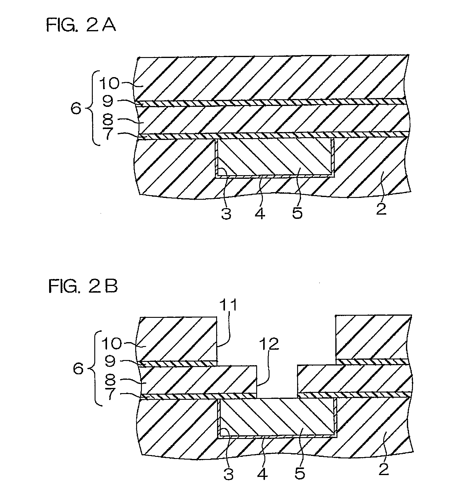
[0046]FIGS. 2A to 2G are schematic sectional views showing the steps of manufacturing the semiconductor device by a method according to the present invention.
[0047]As shown in FIG. 2A, the diffusion preventing film 7, the first interlayer dielectric film 8, the etching stopper film 9 and the second interlayer dielectric film 10 are stacked in this order by CVD (Chemical Vapor Deposition) on the first insulating layer 2 having the first barrier film 4 and the first wire 5 embedded therein. Thus, the second insulating layer 6 is formed on the first insulating layer 2.
[0048]Thereafter the second groove 11 and the via hole 12 are formed in the second insulating layer 6, as shown in FIG. 2B. More specifically, a mask (not shown) having an opening selectively exposing a portion to be provided with the via hole 12 is first formed on the second insulating layer 6. Then, the second interlayer dielectric film 10, the etching stopper film 9 and the first interlayer dielectric film 8 are dry-et...
second embodiment
[0057]FIGS. 3A to 3F are schematic sectional views showing the steps of manufacturing the semiconductor device by a method according to the present invention.
[0058]As shown in FIG. 3A, the diffusion preventing film 7, the first interlayer dielectric film 8, the etching stopper film 9 and the second interlayer dielectric film 10 are stacked in this order by CVD on the first insulating layer 2 having the first barrier film 4 and the first wire 5 embedded therein. Thus, the second insulating layer 6 is formed on the first insulating layer 2.
[0059]Thereafter the second groove 11 and the via hole 12 are formed in the second insulating layer 6, as shown in FIG. 3B. More specifically, a mask (not shown) having an opening selectively exposing a portion to be provided with the via hole 12 is first formed on the second insulating layer 6. Then, the second interlayer dielectric film 10, the etching stopper film 9 and the first interlayer dielectric film 8 are dry-etched through the mask. At th...
third embodiment
[0074]FIGS. 6A to 6E are schematic sectional views showing the steps of manufacturing the semiconductor device by a method according to the present invention. FIG. 7 is a graph showing the relation between an RF bias and coverage of the second groove and the via hole with the alloy film.
[0075]As shown in FIG. 6A, the diffusion preventing film 7, the first interlayer dielectric film 8, the etching stopper film 9 and the second interlayer dielectric film 10 are stacked in this order by CVD on the first insulating layer 2 having the first barrier film 4 and the first wire 5 embedded therein. Thus, the second insulating layer 6 is formed on the first insulating layer 2.
[0076]Thereafter the second groove 11 and the via hole 12 are formed in the second insulating layer 6, as shown in FIG. 6B. More specifically, a mask (not shown) having an opening selectively exposing a portion to be provided with the via hole 12 is first formed on the second insulating layer 6. Then, the second interlaye...
PUM
 Abstract
Description
Claims
Application Information


