Circuit protection device and method of manufacturing the same

Active Publication Date: 2010-02-25
INNOCHIPS TECH
View PDF8 Cites 20 Cited by
  • Summary
  • Abstract
  • Description
  • Claims
  • Application Information

AI Technical Summary

Benefits of technology

[0025]As described above, according to the present invention, a circuit protection device is formed as a single device by laminating a solenoid-type common mode noise filter and an ESD protection device, and the circuit protection device is disposed between a circuit and input/output terminals of an electronic device, so that common mode noises and ESD of the electronic device can be simultaneously prevented using a single chip device.
[0026]As described above, according to the present invention, there is provided a circuit protection device implemented as a single composite device formed by laminating and compressing a common mode noise filter, which has a screw-thread-shaped coil surrounding a magnetic core formed by laminating magnetic layers formed on a plurality of sheets, and an ESD protection device which has an ESD protection material embedded in a plurality of sheets, and a method of manufacturing the circuit protection device; or by laminating and compressing a common mode noise filter and an ESD protection device filled with ESD protection

Problems solved by technology

Because such electronic devices are sensitive to a stimulus from the outside, their circuits may be damaged or signals may be distorted when small abnormal voltages and high-frequency noises are introduced into internal circuits of the electronic devices from the outside.
Switching voltages generated in circuits, power noises contained in power voltages, unnecessary electromagnetic signals, electromagnetic noises, and the like cause such

Method used


Image

  • Circuit protection device and method of manufacturing the same
  • Circuit protection device and method of manufacturing the same
  • Circuit protection device and method of manufacturing the same

Examples


Embodiment Construction

[0043]Hereinafter, exemplary embodiments of the present invention will be described in detail with reference to the accompanying drawings.

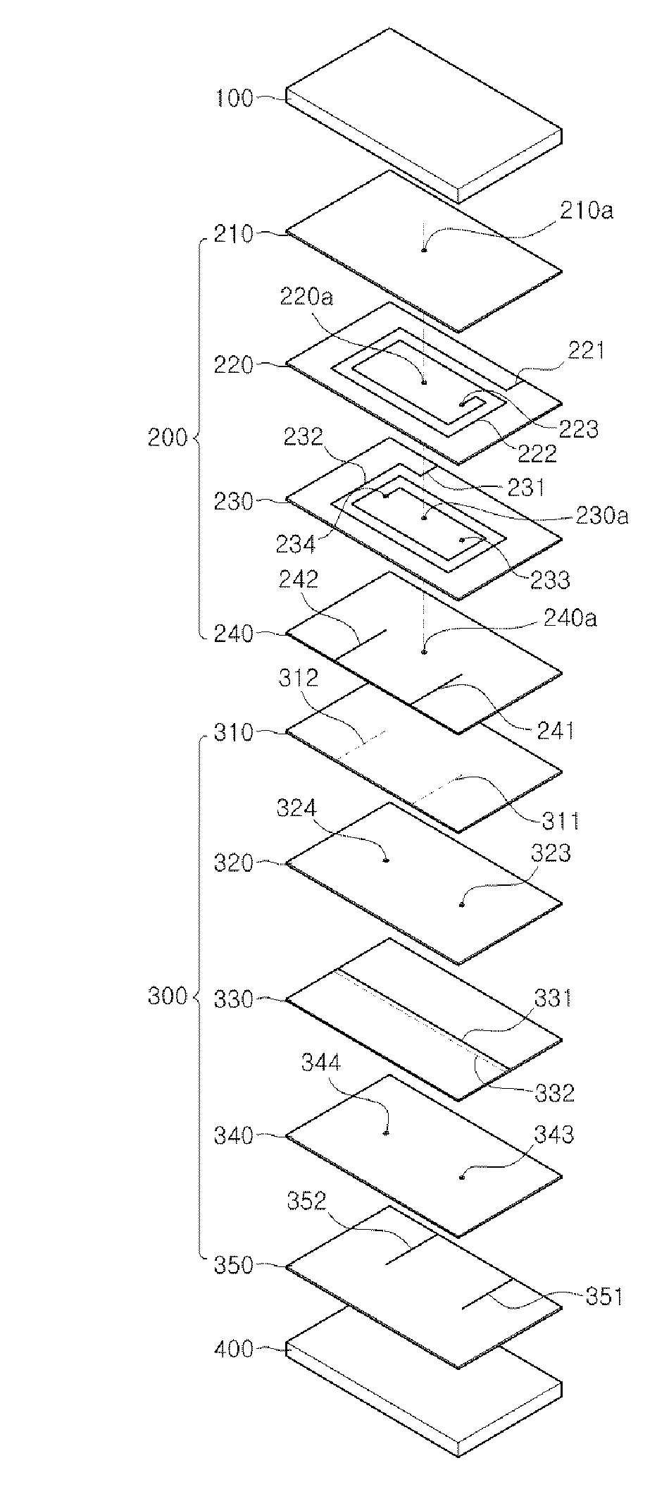
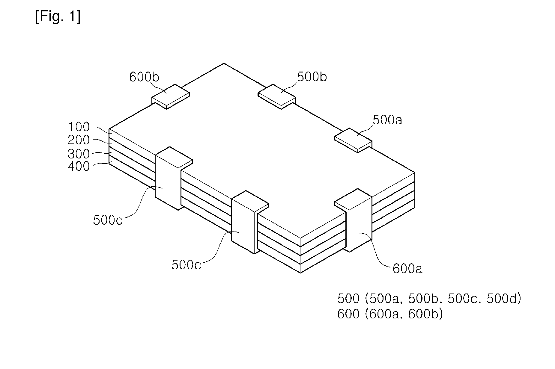
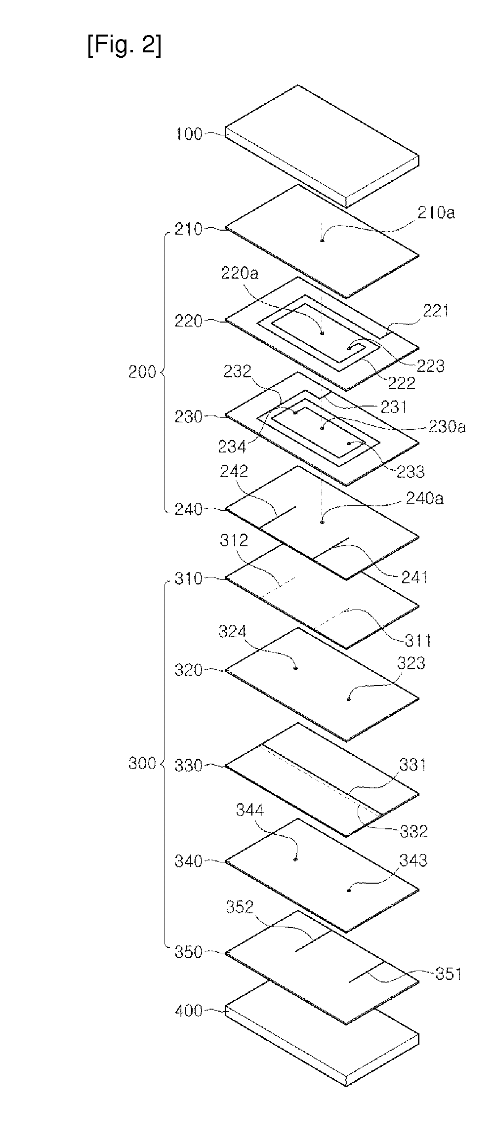
[0044]FIG. 1 is a perspective view showing an assembled state of a circuit protection device according to a first exemplary embodiment of the present invention, and FIG. 2 is an exploded perspective view of the circuit protection device.

[0045]Referring to FIGS. 1 and 2, the circuit protection device according to the first exemplary embodiment of the present invention is formed by laminating a plurality of insulating sheets including an upper cover layer 100, a common mode noise filter 200, an ESD protection device 300 and a lower cover layer 400 from the top. The circuit protection device further includes: external electrodes 500 (500a, 500b, 500c and 500d) connected to some of internal electrodes of the common mode noise filter 200 and some of internal electrodes of the ESD protection device 300; and external electrodes 600 (600a and 600b) connec...


PUM

PropertyMeasurementUnit
Timeaaaaaaaaaa
Capacitanceaaaaaaaaaa
Sizeaaaaaaaaaa

Abstract

The present invention relates to a circuit protection device and a method of manufacturing the same. The circuit protection device includes a common mode noise filter having a plurality of sheets, each of the sheets being formed to optionally include a coil pattern, an internal electrode, a hole filled with a conductive material, and a hole filled with a magnetic material; and an electrostatic discharge (ESD) protection device having a plurality of sheets, each of the sheets being formed to optionally include an internal electrode and a hole filled with an ESD protection material. According to the present invention, a solenoid-type common mode noise filter and an ESD protection device are laminated as a single device, and thereby common mode noises and ESD of the electronic device can be simultaneously prevented. Accordingly, the circuit protection device has a simple configuration as compared with a conventional art in which discrete devices are used to prevent common mode noises and ESD, so that an increase in size of an electronic device can be prevented, and input/output signal distortion can be prevented to thereby enhance the reliability of the electronic device.

Description

TECHNICAL FIELD[0001]The present invention relates to a circuit protection device and a method of manufacturing the same, and more particularly, to a circuit protection device formed as a single composite device by laminating a solenoid-type common mode noise filter and an electro static discharge (hereinafter, referred to as “ESD”) protection device, and a method of manufacturing the circuit protection device.BACKGROUND ART[0002]Recently, electronic devices such as mobile phones, home appliances, PCs, PDAs, LCDs and navigators have been gradually digitalized and operated at high speed. Because such electronic devices are sensitive to a stimulus from the outside, their circuits may be damaged or signals may be distorted when small abnormal voltages and high-frequency noises are introduced into internal circuits of the electronic devices from the outside.[0003]Switching voltages generated in circuits, power noises contained in power voltages, unnecessary electromagnetic signals, elec...

Claims


Application Information

Patent Timeline
IPC IPC(8): H02H9/00B32B38/04B29C65/00H03H7/00
CPCH01F17/0033H03H2001/0085H03H7/427H03H7/0107H01L21/02Y10T156/1056H01F27/402H01F2027/2809H05K9/0067Y10T156/1052H01F27/2804
Inventor PARK, IN-KILNOH, TAE-HYUNGJANG, KYU CHEOLLEE, MYUNG HOKIM, GYEONG TAELEE, SANG HWAN
Owner INNOCHIPS TECH
Why Eureka
Try Eureka