Organic light emitting diode display and fabricating method thereof
- Summary
- Abstract
- Description
- Claims
- Application Information
AI Technical Summary
Benefits of technology
Problems solved by technology
Method used
Image

Examples
first embodiment
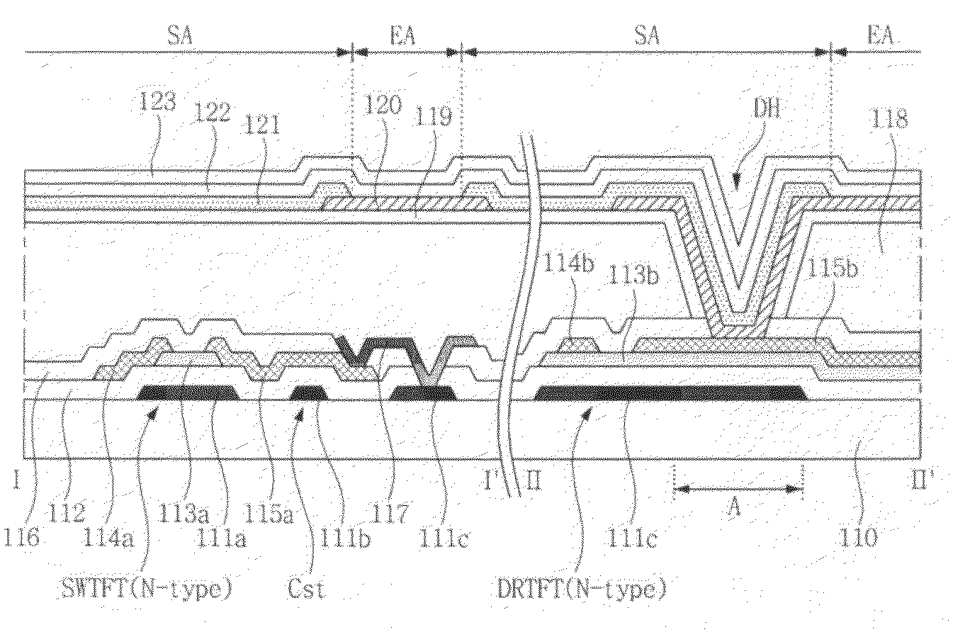
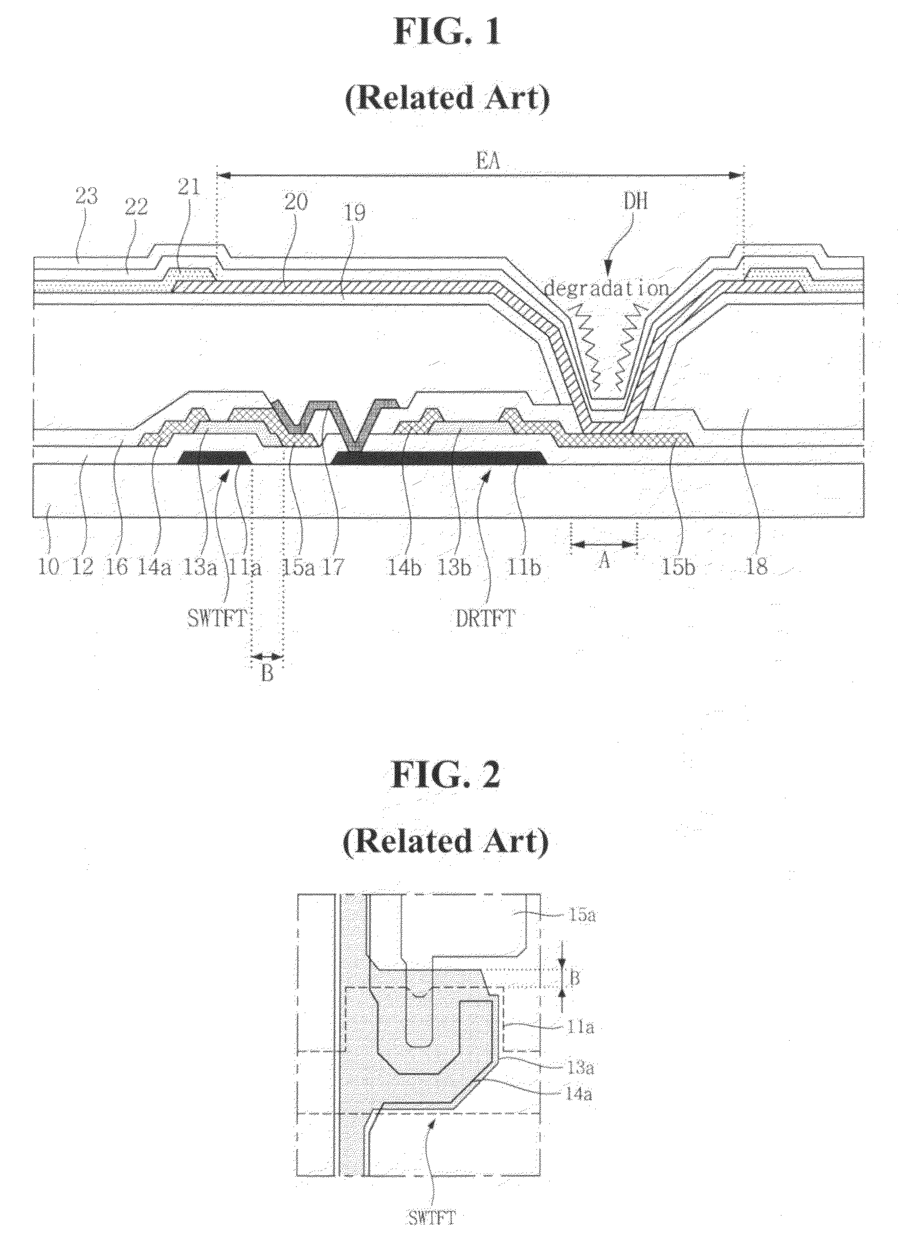
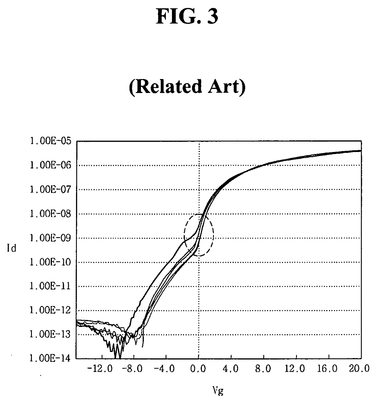
[0046]FIG. 4 illustrates the plane structure of a pixel in the OLED display device according to the present disclosure. FIG. 5 illustrates the cross-sectional structures cutting alone I-I′ line and II-II′ line in FIG. 4. And, FIG. 6 illustrates the equivalent circuit diagram of a pixel in the OLED display device shown in FIG. 5. In FIGS. 4 and 5, the gate pad, the data pad, VDD supply pad and VSS supply pad are not shown, in convenience.
[0047]Referring to FIGS. 4 to 6, the OLED display device according to the first embodiment of the present disclosure comprises the gate line (GL), the data line (DL), VSS supply line 111n, switch TFT (SWTFT), drive TFT (DRTFT), storage capacitor (Cst), overcoat layer 118, buffer layer 119, bank pattern 121, and organic light emitting diode (or “OLED”) formed on a substrate 110. The OLED includes the cathode electrode 120, the organic layer 122, and the anode electrode 123.
[0048]The gate line (GL) is connected to the gate driver through the gate pad s...
second embodiment
[0069]FIG. 20 illustrates a cross-sectional structure of a pixel in the OLED display device according to the present disclosure. FIG. 21 illustrates the equivalent circuit diagram of a pixel in the OLED display device shown in FIG. 20.
[0070]Referring to FIGS. 20 and 21, the OLED display device according to the second embodiment of the present disclosure comprises the gate line (GL), data line (DL), VDD supply line 211b, switch TFT (SWTFT), drive TFT (DRTFT), storage capacitor (Cst), overcoat layer 118, buffer layer 118, bank pattern 121, and OLED on the substrate 110. The OLED includes the reflection electrode 220, anode electrode 21, organic layer 222, and transparent cathode electrode 223.
[0071]The OLED display device according to the second embodiment of the present disclosure is substantially same as the OLED display device according to the first embodiment except that the TFTs (SWTFT and DRTFT) is the P-type MOSFET, the one electrode of the storage capacitor (Cst) is the VDD su...
PUM
 Abstract
Description
Claims
Application Information
 - Generate Ideas
- Intellectual Property
- Life Sciences
- Materials
- Tech Scout
- Unparalleled Data Quality
- Higher Quality Content
- 60% Fewer Hallucinations
Browse by: Latest US Patents, China's latest patents, Technical Efficacy Thesaurus, Application Domain, Technology Topic, Popular Technical Reports.
© 2025 PatSnap. All rights reserved.Legal|Privacy policy|Modern Slavery Act Transparency Statement|Sitemap|About US| Contact US: help@patsnap.com