Epitaxial substrate, semiconductor device substrate, and HEMT device

a technology of semiconductor devices and substrates, applied in the direction of semiconductor devices, basic electric elements, electrical equipment, etc., to achieve the effect of excellent characteristics

Active Publication Date: 2010-03-04
NGK INSULATORS LTD
View PDF15 Cites 17 Cited by
  • Summary
  • Abstract
  • Description
  • Claims
  • Application Information

AI Technical Summary

Benefits of technology

[0010]Thereby, the epitaxial substrate capable of laminating functional layers formed of a group III nitride having preferable crystal quality without causing cracks can be obtained.
[0012]Thereby, when functional layers are formed on the epitaxial substrate, FET having excellent characteristics with mobility of at least 1300 cm2 / Vs and drain current of at least 1000 mA / mm can be manufactured.
[0015]It is therefore an object of the present invention to provide an epitaxial substrate capable of fabricating an electronic device having excellent characteristics, and an electronic device manufactured by using the same.

Problems solved by technology

However, National Publication of Translation No. 2002-520880 and Japanese Patent Application Laid-Open No. 2006-286741 do not disclose any of the relationship of a specific formation of an AlN film functioning as a buffer layer to crystal quality of a GaN film, and further to a characteristics of an electronic device configured to form a functional layer with the GaN film or the like.

Method used


Image

  • Epitaxial substrate, semiconductor device substrate, and HEMT device
  • Epitaxial substrate, semiconductor device substrate, and HEMT device
  • Epitaxial substrate, semiconductor device substrate, and HEMT device

Examples


example

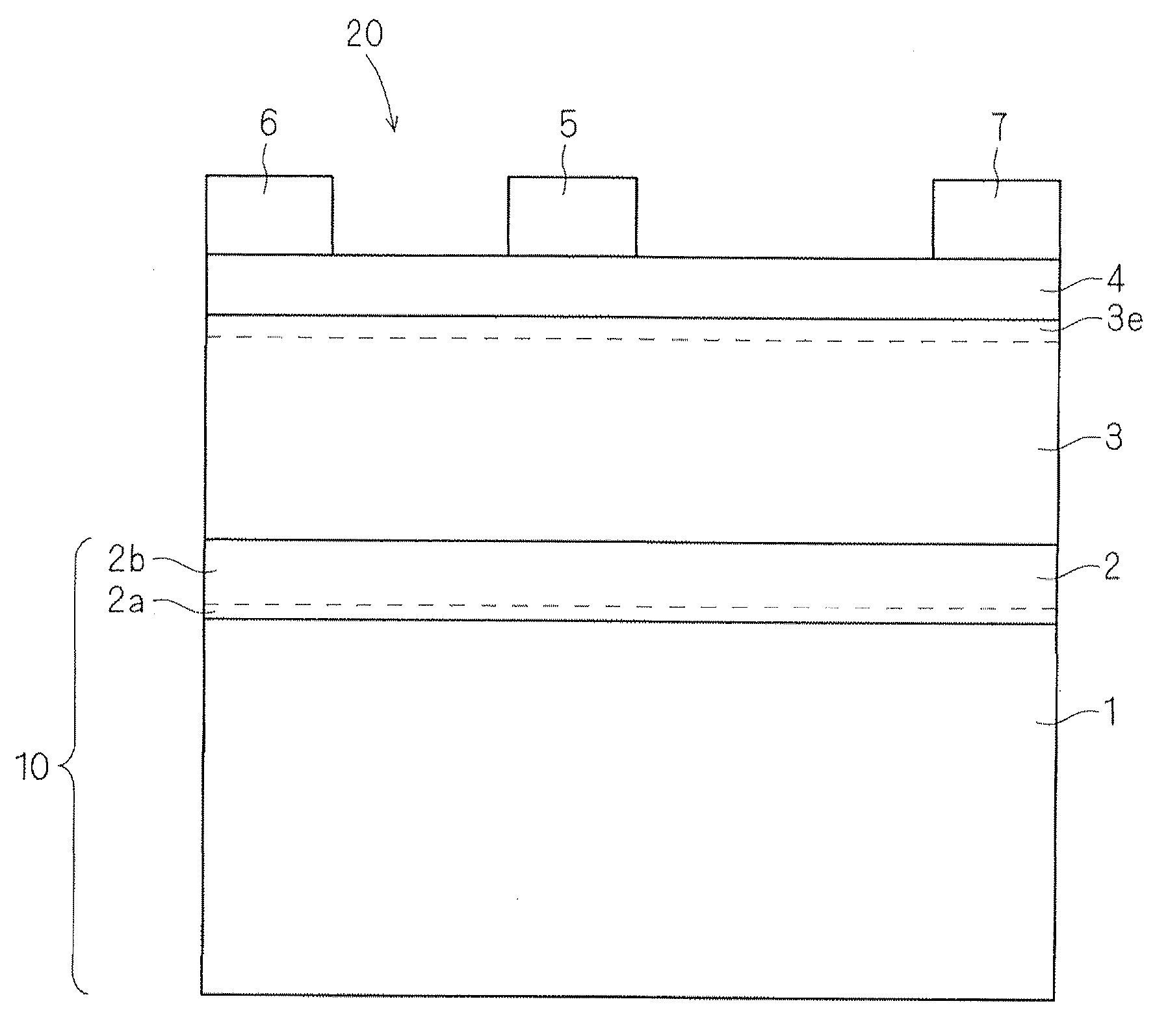
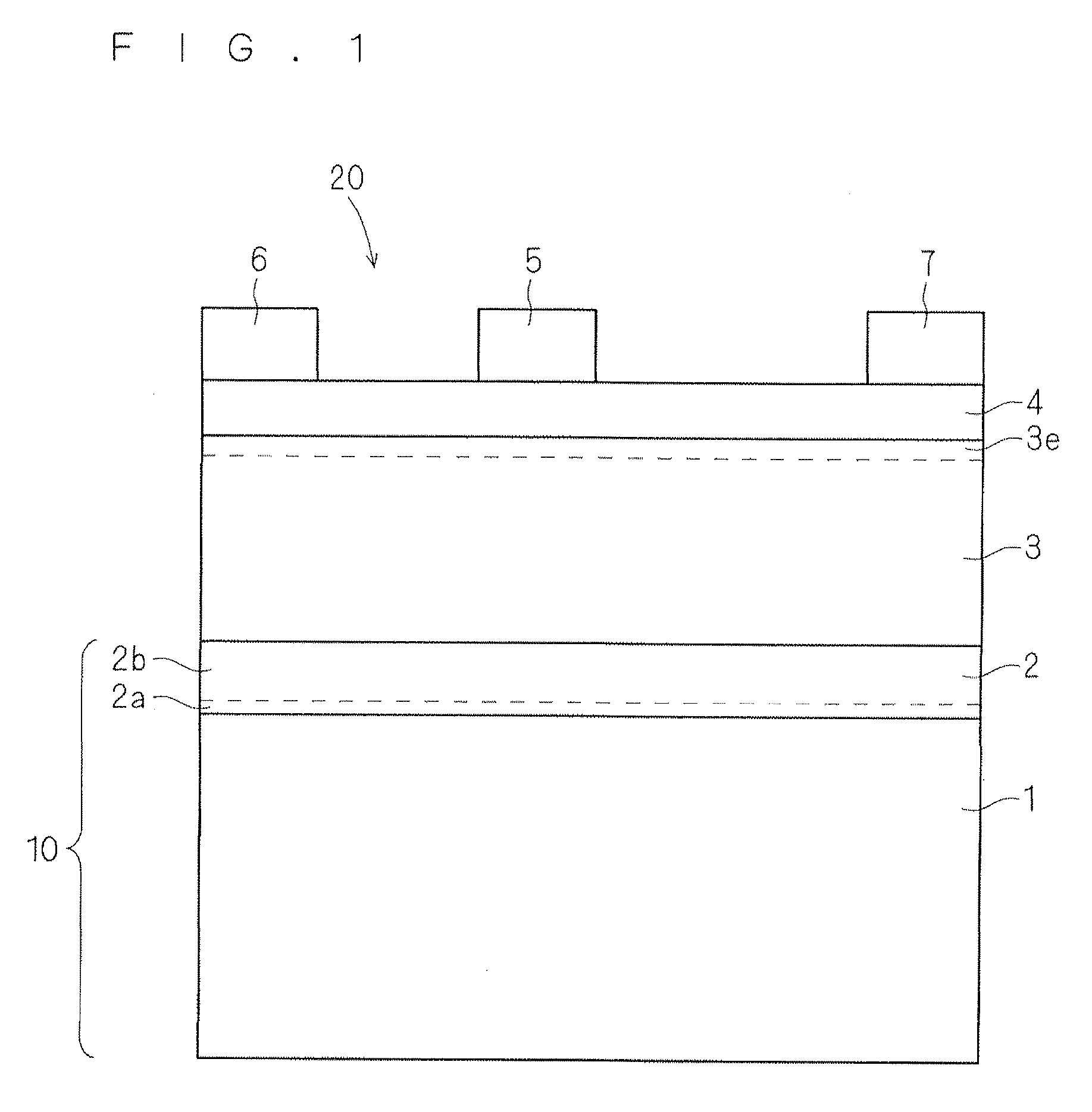
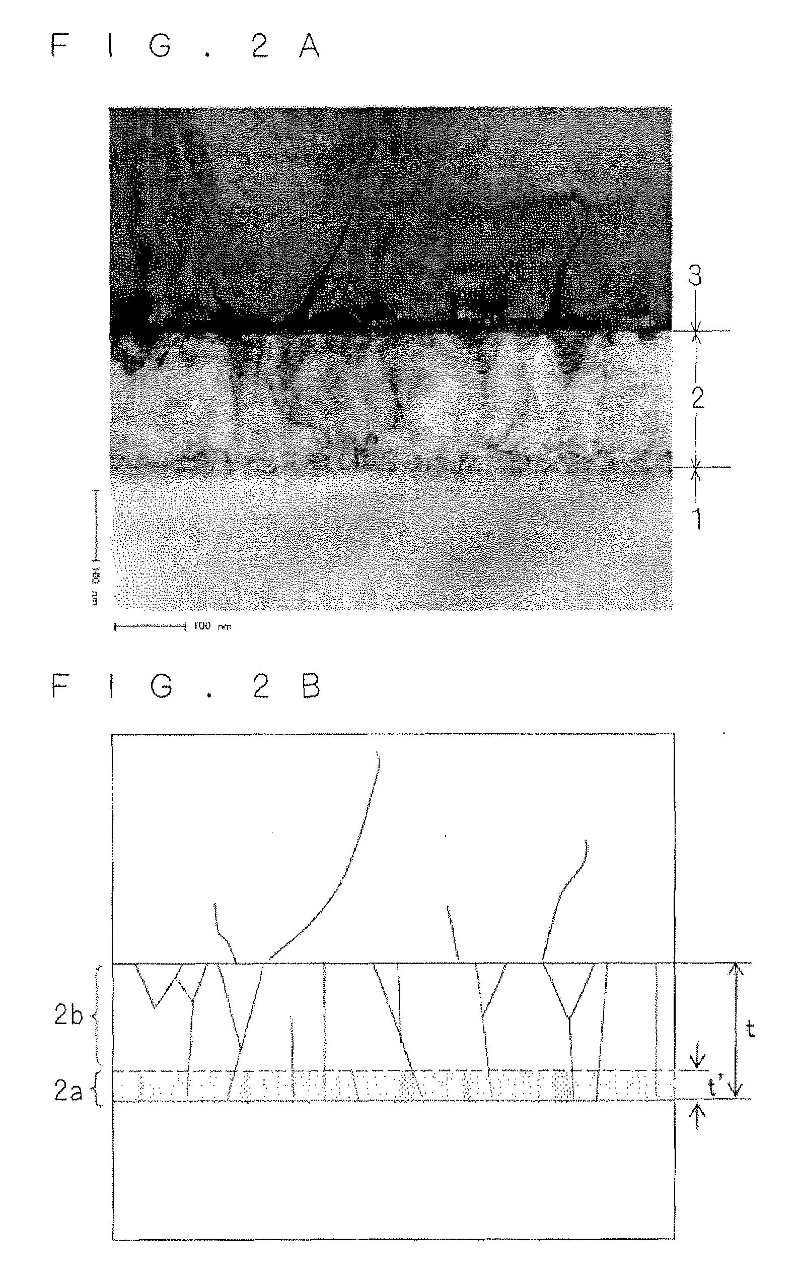
[0072]A plurality of semi-insulating single crystal 6H—SiC bases were prepared as the base 1, and an AlN layer was formed as the buffer layer 2 by an MOCVD method, to fabricate 18 types of a plurality of epitaxial substrates 10, each type corresponding to No. 1 to No. 18 in FIG. 6. Specifically, each of the 6H—SiC bases was set in a susceptor inside a reactor of a well-known MOCVD furnace, and was heated by the susceptor while the AlN layer was formed by introducing TMA (trimethyl aluminum) as an Al source gas into the reactor by bubbling of hydrogen gas, with ammonia gas flowing, and hydrogen gas being used as a carrier gas. The flow volume of ammonia gas was 3000 sccm. Eighteen types of samples were obtained by variously setting the temperature of the susceptor within the range between 1050° C. and 1250° C., the pressure inside the reactor within the range between 50 Torr and 200 Torr, and setting the thickness of the AlN layer to be one of 100 nm, 200 nm, and 300 nm.

[0073]Further...


PUM


Abstract

A buffer layer formed of Inx1Aly1Gaz1N formed on a base, with an upper part of the buffer layer containing columnar polycrystalline including a grain boundary existing in a direction substantially perpendicular to a surface of the base. The number of grain boundaries in the lower part of the buffer layer is greater than that in the upper part, and a full width at half maximum of an X-ray rocking curve of the upper part is 300-3000 seconds, RMS of the surface of the buffer layer is 0.2 nm-6 nm, and the ratio of the grain boundary width of the crystal grain of the upper part in a direction parallel to the base surface to the formation thickness of the buffer layer is 0.5-1.5.

Description

BACKGROUND OF THE INVENTION[0001]1. Field of the Invention[0002]The present invention relates to an epitaxial substrate prepared by epitaxially growing a group III nitride semiconductor on an SiC base, and to an HEMT device using the same.[0003]2. Description of the Background Art[0004]Nitride semiconductors having higher breakdown electric field and higher electron saturation velocities have been drawing attention as semiconductor materials for high-frequency and high-power devices. In manufacturing such devices, a group III nitride semiconductor is generally epitaxially grown on a predetermined base substrate. While an SiC substrate, a sapphire substrate or the like is mainly used as a base substrate, defect density of the group III nitride semiconductor grown thereon can be much more reduced (crystal quality is further improved) when using the SiC substrate than when using the sapphire substrate since SiC has a lattice constant closer to AlN and GaN than sapphire. Further, an SiC...

Claims


Application Information

Patent Timeline
Patent Type & Authority Applications(United States)
IPC IPC(8): H01L29/778H01L29/24
CPCH01L21/02378H01L21/02458H01L21/02513H01L21/0254H01L29/7787H01L29/2003H01L29/267H01L29/66462H01L29/1608
Inventor KURAOKA, YOSHITAKAMIYOSHI, MAKOTOSUMIYA, SHIGEAKITANAKA, MITSUHIRO
Owner NGK INSULATORS LTD
Why Eureka
Try Eureka