Method to improve dielectric quality in high-k metal gate technology

a metal gate and dielectric quality technology, applied in the field of high-k metal gate technology, can solve the problems of gate dielectric, increased complexity of processing and manufacturing ics, and gate dielectric problems

Active Publication Date: 2010-03-04
TAIWAN SEMICON MFG CO LTD
View PDF1 Cites 23 Cited by
  • Summary
  • Abstract
  • Description
  • Claims
  • Application Information

AI Technical Summary

Benefits of technology

[0003]In the course of IC evolution, functional density (i.e., the number of interconnected devices per chip area) has generally increased while geometry size (i.e., the smallest component (or line) that can be created using a fabrication process) has decreased. This scaling down process generally provides benefits by increasing production efficiency and lowering associated costs. Such scaling-down also produces a relatively high power dissipation value, which may be addressed by using low power dissipation devices such as complementary metal-oxide-semiconductor (CMOS) devices. CMOS devices have typically been formed with a gate oxide and polysilicon gate electrode. There has been a desire to replace the gate oxide and polysilicon gate electrode with a high-k gate dielectric and metal gate electrode to improve device performance as feature sizes continue to decrease. However, problems arise when integrating a high-k / metal gate feature in a CMOS process flow due to various factors such as incompatibility of materials, complex processes, and thermal budgets. For example, one of the issues for high-k gate dielectric is its lower thermal stability. Accordingly, a quality of the high-k gate dielectric may change during a thermal process cycle and surrounding environment of the CMOS process flow, and thus may result in poor device performance and reliability.
[0063]The present invention achieves different advantages in various embodiments disclosed herein. For example, the present disclosed method provides a simple and cost-effective method for improving a dielectric quality of a high-k gate dielectric in a CMOS process flow. Accordingly, the integrity of the high-k gate dielectric may be maintained throughout semiconductor processing. The methods and devices disclosed herein may easily be integrated with current CMOS technology processing and semiconductor equipment. Further, the methods and devices disclosed herein lessen the dimension dependence of device performance characteristics such as threshold voltage, drive-current, and off-current.

Problems solved by technology

However, these advances have increased the complexity of processing and manufacturing ICs and, for these advances to be realized, similar developments in IC processing and manufacturing are needed.
However, problems arise when integrating a high-k / metal gate feature in a CMOS process flow due to various factors such as incompatibility of materials, complex processes, and thermal budgets.
For example, one of the issues for high-k gate dielectric is its lower thermal stability.
Accordingly, a quality of the high-k gate dielectric may change during a thermal process cycle and surrounding environment of the CMOS process flow, and thus may result in poor device performance and reliability.

Method used


Image

  • Method to improve dielectric quality in high-k metal gate technology
  • Method to improve dielectric quality in high-k metal gate technology
  • Method to improve dielectric quality in high-k metal gate technology

Examples


Embodiment Construction

[0015]It is to be understood that the following disclosure provides many different embodiments, or examples, for implementing different features of the invention. Specific examples of components and arrangements are described below to simplify the present disclosure. These are, of course, merely examples and are not intended to be limiting. Moreover, the formation of a first feature over or on a second feature in the description that follows may include embodiments in which the first and second features are formed in direct contact, and may also include embodiments in which additional features may be formed interposing the first and second features, such that the first and second features may not be in direct contact. Various features may be arbitrarily drawn in different scales for simplicity and clarity.

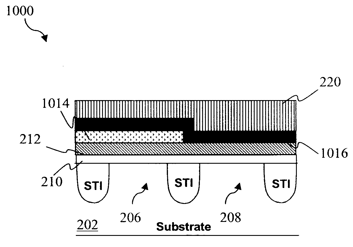
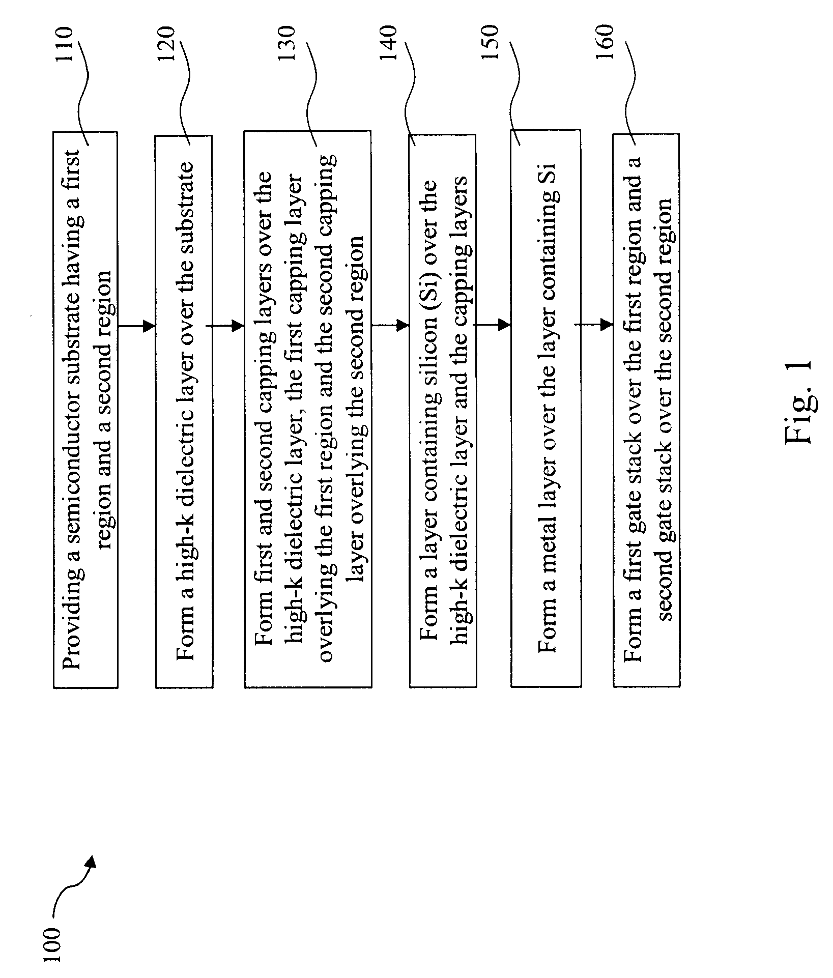
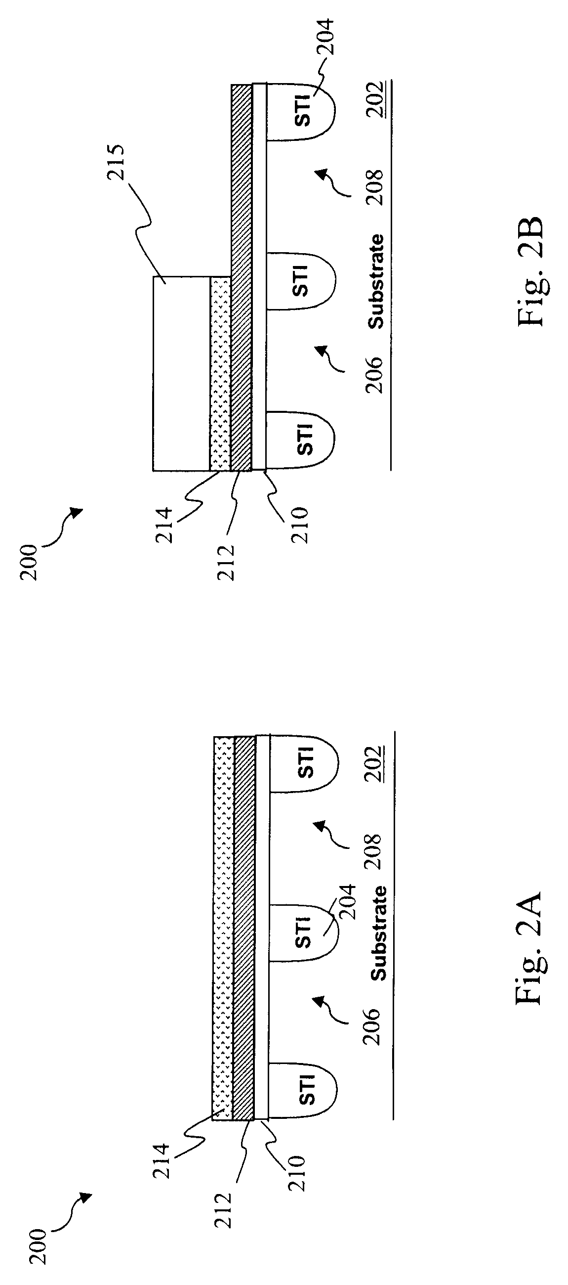
[0016]Referring to FIG. 1, illustrated is a flowchart of a method 100 for fabricating a semiconductor device having a high-k dielectric and metal gate according to various aspects ...


PUM


Abstract

The present disclosure provides a method of fabricating a semiconductor device. The method includes providing a semiconductor substrate having a first active region and a second active region, providing a semiconductor substrate having a first region and a second region, forming a high-k dielectric layer over the semiconductor substrate, forming a first capping layer and a second capping layer over the high-k dielectric layer, the first capping layer overlying the first region and the second capping layer overlying the second region, forming a layer containing silicon (Si) over the first and second capping layers, forming a metal layer over the layer containing Si, and forming a first gate stack over the first region and a second gate stack over the second active region. The first gate stack includes the high-k dielectric layer, the first capping layer, the layer containing Si, and the metal layer and the second gate stack includes the high-k dielectric layer, the second capping layer, the layer containing Si, and the metal layer.

Description

PRIORITY DATA[0001]This application claims priority to U.S. Provisional Application Ser. No. 61 / 092,616, filed on Aug. 28, 2008, entitled “METHOD TO IMPROVE DIELECTRIC QUALITY IN HIGH-K METAL GATE TECHNOLOGY,” the entire disclosure of which is incorporated herein by reference.BACKGROUND[0002]The semiconductor integrated circuit (IC) industry has experienced rapid growth. Technological advances in IC materials and design have produced generations of ICs where each generation has smaller and more complex circuits than the previous generation. However, these advances have increased the complexity of processing and manufacturing ICs and, for these advances to be realized, similar developments in IC processing and manufacturing are needed.[0003]In the course of IC evolution, functional density (i.e., the number of interconnected devices per chip area) has generally increased while geometry size (i.e., the smallest component (or line) that can be created using a fabrication process) has d...

Claims


Application Information

Patent Timeline
Patent Type & Authority Applications(United States)
IPC IPC(8): H01L25/11H01L21/4763H01L29/78
CPCH01L21/28061H01L21/28185H01L21/28194H01L29/517H01L29/4925H01L29/513H01L21/823842
Inventor MASUOKA, YURIHSU, PENG-FUHUANG, HUAN-TSUNGHUANG, KUO-TAIDIAZ, CARLOS H.HOU, YONG-TIAN
Owner TAIWAN SEMICON MFG CO LTD
Why Eureka
Try Eureka