Self-aligning metal oxide thin film transistor and manufacturing method thereof

A technology of oxide film and production method, which is applied in transistor, semiconductor/solid-state device manufacturing, electrical components and other directions, can solve the problems of self-aligned structure stability, production efficiency and cost, production line compatibility, etc. Improved on-state current and mobility, low cost, reduced overlap capacitance

Inactive Publication Date: 2013-09-18
PEKING UNIV SHENZHEN GRADUATE SCHOOL
View PDF3 Cites 16 Cited by
  • Summary
  • Abstract
  • Description
  • Claims
  • Application Information

AI Technical Summary

Problems solved by technology

The methods of realizing self-aligned thin-film transistors that have been reported have many disadvantages, such as: compatibility with traditional large-area panel production lines, self-aligned structure stability, manufacturing efficiency and cost issues, etc.

Method used


Image

  • Self-aligning metal oxide thin film transistor and manufacturing method thereof
  • Self-aligning metal oxide thin film transistor and manufacturing method thereof
  • Self-aligning metal oxide thin film transistor and manufacturing method thereof

Examples


Embodiment 1

[0069] A specific example of the manufacturing method of the thin film transistor of the present invention is as follows Figure 1 to Figure 7 shown, including the following steps:

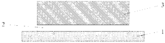
[0070] Such as figure 1 As shown, the substrate 1 used is a glass substrate, and a 60nm metal oxide semiconductor indium gallium zinc oxide (IGZO) thin film 2 is grown on the substrate by magnetron sputtering.

[0071] Such as figure 2 As shown, the photoresist 3 is spin-coated, and the indium gallium zinc oxide thin film 2 is photolithographically etched; the photoresist 3 is removed by ultrasonication with acetone.

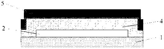
[0072] Such as image 3 As shown, a 200nm silicon oxide film 4 is deposited on the patterned indium gallium zinc oxide film 2 by plasma enhanced chemical vapor deposition (PECVD); then a 150nm silicon oxide film is grown by magnetron sputtering Metal molybdenum film 5.

[0073] Such as Figure 4 As shown, the photoresist 6 is spin-coated, the molybdenum electrode and the sil...

Embodiment 2

[0078] Another specific example of the manufacturing method of the thin film transistor of the present invention is as follows Figure 8 to Figure 15 shown, including the following steps:

[0079] Such as Figure 8 As shown, the substrate 1 used is a glass substrate, and a layer of 80nm metal oxide semiconductor indium gallium zinc oxide (IGZO) thin film 2 is grown on the substrate by magnetron sputtering.

[0080] Such as Figure 9 As shown, the photoresist 3 is spin-coated, and the indium gallium zinc oxide thin film 2 is photolithographically etched; the photoresist 3 is removed by ultrasonication with acetone.

[0081] Such as Figure 10As shown, a layer of 300nm silicon oxide film 4 is deposited on the patterned indium gallium zinc oxide film 2 by plasma enhanced chemical vapor deposition (PECVD); then a layer of 300nm silicon oxide film is grown by magnetron sputtering Metal molybdenum film 5.

[0082] Such as Figure 11 As shown, the photoresist 6 is spin-coated, ...

Embodiment 3

[0088] Another specific example of the manufacturing method of the thin film transistor of the present invention is as follows Figure 16 to Figure 22 shown, including the following steps:

[0089] Such as Figure 16 As shown, the substrate 1 used is a flexible substrate, and a layer of 40nm high-resistivity metal oxide semiconductor indium gallium zinc oxide (IGZO) film 2 is grown on the substrate by magnetron sputtering; and then grown by magnetron sputtering A 5nm low-resistivity indium tin oxide film (ITO) 17 .

[0090] Such as Figure 17 As shown, the photoresist 3 is spin-coated, the indium gallium zinc oxide thin film 2 and the indium tin oxide thin film 17 are photolithographically and etched; the photoresist 3 is removed by ultrasonication with acetone.

[0091] Such as Figure 18 As shown, a 100nm aluminum oxide film 4 is deposited on the patterned indium tin oxide film 17 by atomic layer deposition (ALD); then a 50nm metal molybdenum film 5 is grown by magnetron...


PUM

PropertyMeasurementUnit
thicknessaaaaaaaaaa
thicknessaaaaaaaaaa
thicknessaaaaaaaaaa

Abstract

The invention provides a self-aligning metal oxide thin film transistor and a manufacturing method thereof. The method includes depositing a metal oxide semiconductor layer, a gate dielectric layer and a conducting thin film on a substrate and photoetching for imaging, spin-coating a dopant layer on the surface of a device, performing heat treatment to enable doping atoms in the spin-coated dopant layer to be diffused into a lower-layer material. The graphical gate electrode and the graphic gate dielectric exist, so that the doping atoms can only be diffused into metal oxide semiconductor areas on two sides of a channel area, doping of the metal oxide semiconductor on two sides of a channel is realized, resistivity of the metal oxide semiconductor is greatly lowered, and a self-aligned source-drain area is formed. The spin-coated dopant layer can also serve as a passivating layer of the device and is combined with subsequent processes like photoetching of contact holes and leading-out of electrodes and a wiring layer to manufacture a complete TFT (thin film transistor) device. The metal oxide thin film transistor prepared by the method has a self-aligning structure and is simple in process and compatible with large-area substrate process.

Description

technical field [0001] The invention relates to a thin film transistor and a preparation method thereof, in particular to a metal oxide thin film transistor with a top gate self-aligned structure and a preparation method thereof. Background technique [0002] As a type of MOS device, thin-film transistors (TFTs: thin-film transistors) have always been the core device of flat panel display, which are mainly used in the switch control of pixel circuit of flat panel display panel, driving of pixel circuit and peripheral driving circuit of display panel. In addition, thin film transistors are also widely used in sensors, memories, processors and other fields. Thin film transistors can be divided into many types according to the different materials of the active layer, including traditional silicon-based thin film transistors, metal oxide thin film transistors (Oxide TFTs) and organic thin film transistors (Organic TFTs). Among the various thin film transistors made of different...

Claims


Application Information

Patent Timeline
Patent Type & Authority Applications(China)
IPC IPC(8): H01L21/336H01L21/228H01L29/786
Inventor 张盛东肖祥迟世鹏
Owner PEKING UNIV SHENZHEN GRADUATE SCHOOL
Why Eureka
Try Eureka