MEMS structure and method for fabricating the same

Active Publication Date: 2010-03-04
MARLIN SEMICON LTD
View PDF6 Cites 13 Cited by
  • Summary
  • Abstract
  • Description
  • Claims
  • Application Information

AI Technical Summary

Benefits of technology

[0008]The present invention is directed to a method for fabricating the MEMS, by which MEMS devices may be integrated with a CMOS process to reduce the fabricating procedures.
[0025]As mentioned above, the MEMS structure of the present invention includes the protection rings and the dielectric layers to connect two adjacent metal layers, and the residue stress in the metal layers can thus be reduced, thereby the bending problem of the metal layers can be solved. Additionally, since the metal layers and the protection rings constitute a large-area conductor structure, the induced capacitance and the mass can be increased, so as to enhance the sensitivity and the performance of the MEMS.
[0026]Moreover, the method for fabricating the MEMS can integrated with the CMOS process, such that the fabricating procedures can be simplified and the throughput can be increased. Hence, the roughness, stress and particle issues impacting on the device can also be improved effectively.

Problems solved by technology

The MEMS device easily suffers from the stress issue due to the structure formed from polysilicon material.
Moreover, polysilicon material is prone to bend under an influence of continuously repeating mechanical stress, such that the life of the device is diminished and the performance thereof is unsatisfying.
Accordingly, the formation of the MEMS structure utilizing polysilicon as material needs additional procedures, and the fabricating steps and the cost are raised.
In practical proceeding, the MEMS structure utilized polysilicon material is also limited to the thickness of the polysilicon layer deposited, which makes a great impact on the device.

Method used


Image

  • MEMS structure and method for fabricating the same
  • MEMS structure and method for fabricating the same
  • MEMS structure and method for fabricating the same

Examples


Embodiment Construction

[0030]Reference will now be made in detail to the present preferred embodiments of the invention, examples of which are illustrated in the accompanying drawings. Wherever possible, the same reference numbers are used in the drawings and the description to refer to the same or like parts.

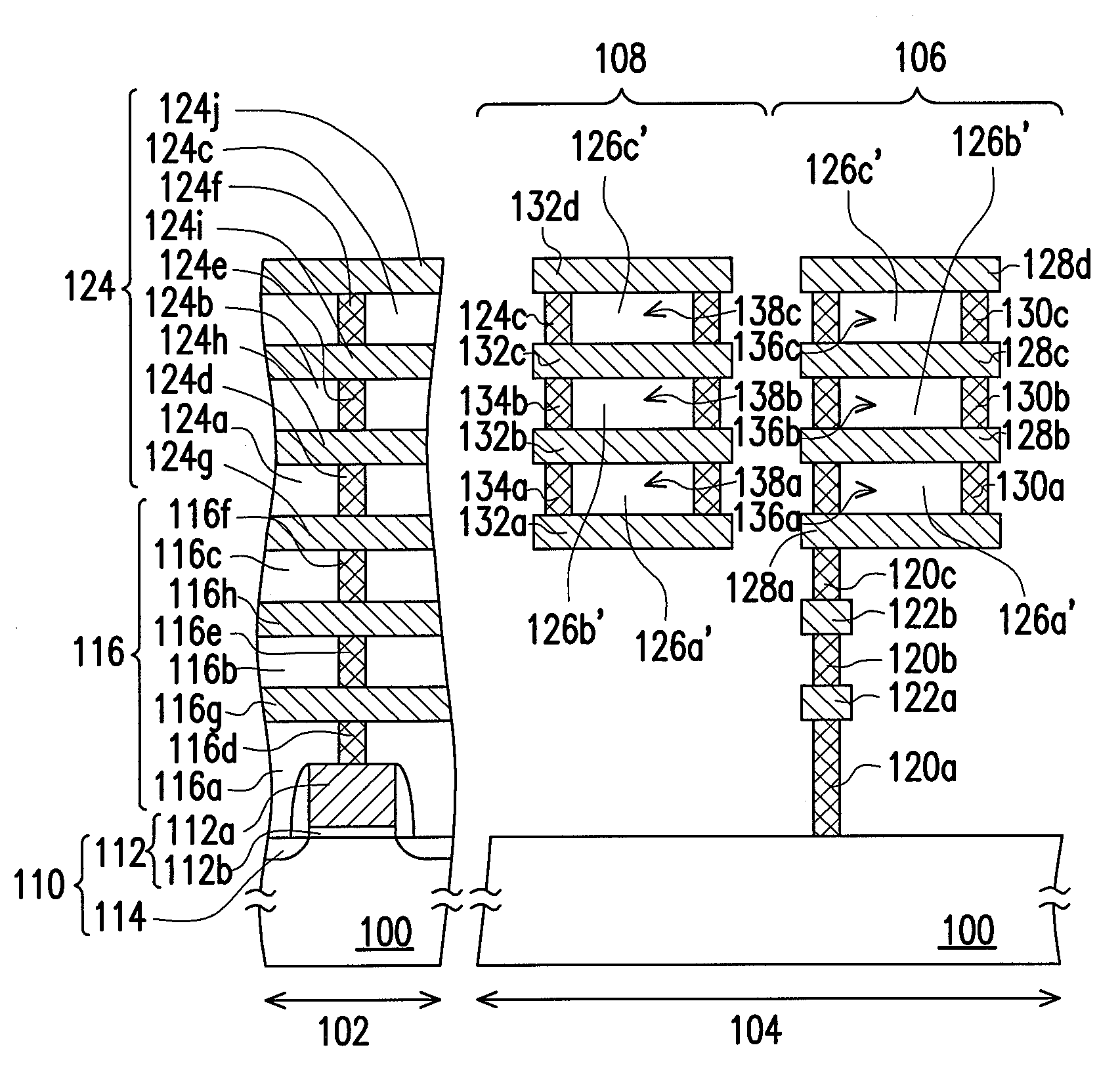
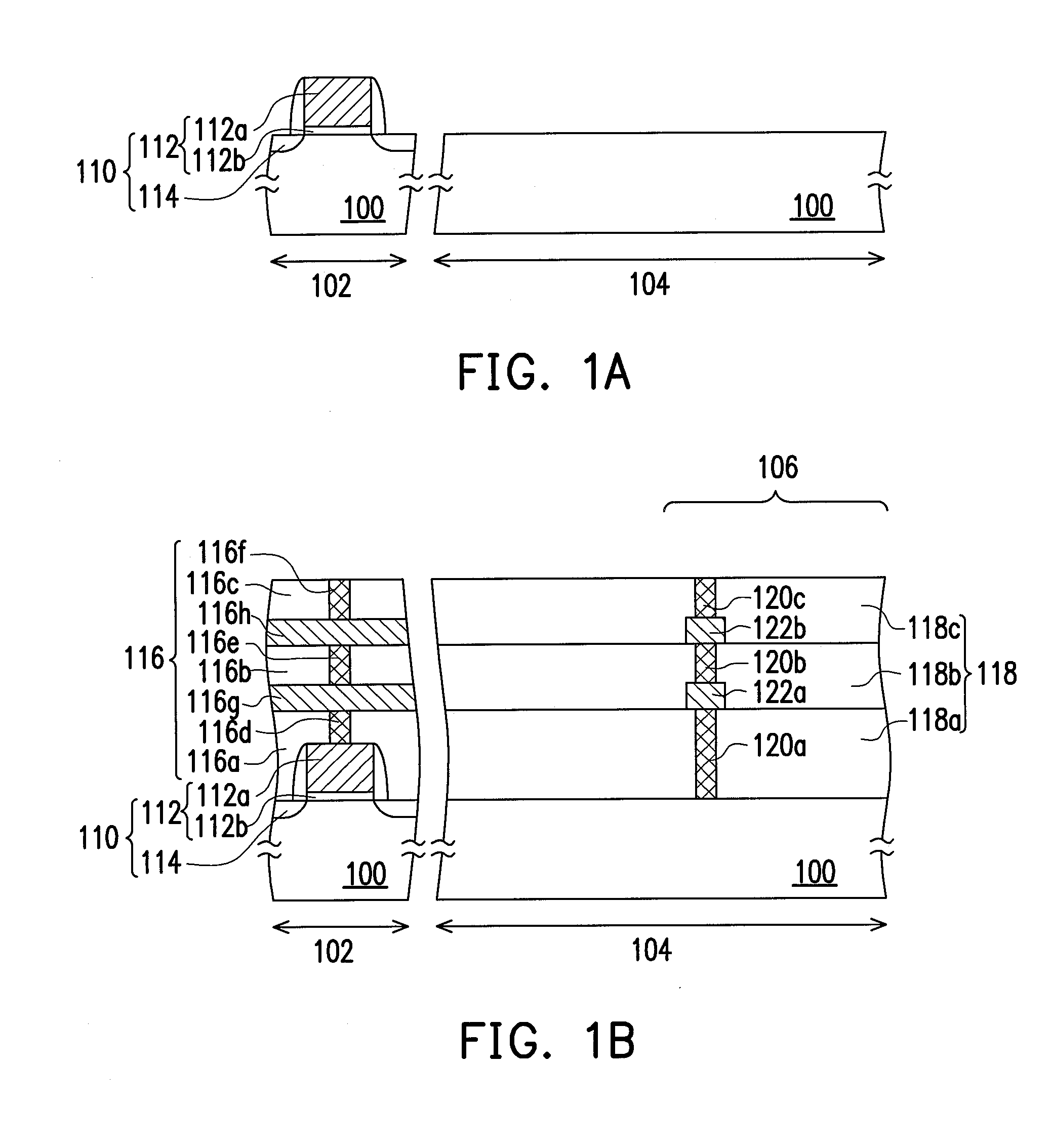
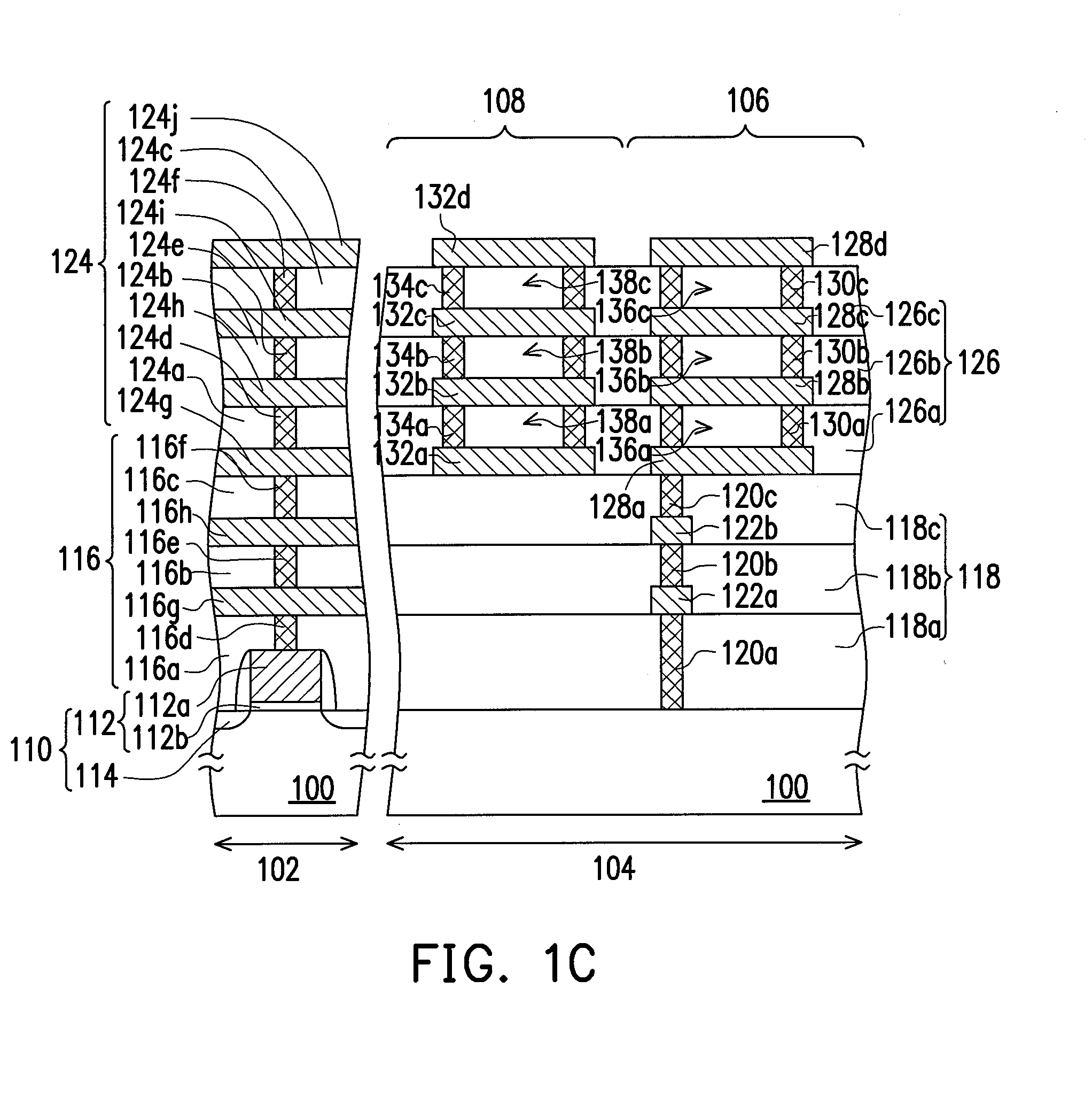
[0031]FIGS. 1A-1D depict, in a cross-sectional view, a method for fabricating an MEMS structure according to an embodiment of this invention. The fabrication of the MEMS structure in the present invention may be integrated with the back end of the CMOS process, so as to simplify manufacturing procedures. Therefore, in the following embodiments, the procedures for fabricating the CMOS transistor, the interconnection process, and the MEMS process are incorporated at the same time to illustrate the present invention.

[0032]Referring to FIG. 1A, a substrate 100 is provided, which may be a semiconductor wafer, e.g. an N-type silicon wafer, a P-type silicon wafer, etc. The substrate 100 includes a circuit r...


PUM

PropertyMeasurementUnit
Timeaaaaaaaaaa
Dielectric polarization enthalpyaaaaaaaaaa

Abstract

A microelectromechanical system (MEMS) structure and a fabricating method thereof are described. The MEMS structure includes a fixed part and a movable part. The fixed part is disposed on and connects with a substrate. The movable part including at least two first metal layers, a first protection ring and a first dielectric layer is suspended on the substrate. The first protection ring connects two adjacent first metal layers, so as to define a first enclosed space between the two adjacent first metal layers. The first dielectric layer is disposed in the enclosed space and connects the two adjacent first metal layers.

Description

BACKGROUND OF THE INVENTION[0001]1. Field of the Invention[0002]The present invention generally relates to a microelectromechanical system (MEMS) structure and a fabricating method thereof, and in particular, to an MEMS structure having a protection ring and a fabricating method thereof.[0003]2. Description of Related Art[0004]A microelectromechanical system (MEMS) is a microelectromechanical device fabricated in a microminiaturized package structure, and the fabricating technique thereof is quite similar to the technique of fabricating integrated circuits (ICs). However, interactions, for example, about mechanics, optics, or magnetic force between the MEMS device and surrounding environment are more than that of the conventional IC. The MEMS device may include micro-sized electromechanical components, such as motors, pumps, valves, switches, capacitors, accelerometers, sensors, capacitive sensors, pixels, microphones, or actuators, etc. The electromechanical components, which are d...

Claims


Application Information

Patent Timeline
IPC IPC(8): H01L23/52H01L21/4763
CPCB81C1/00246B81C2203/0742Y10T29/41Y10T29/49155B81C2203/0714
Inventor LAN, BANG-CHIANGWANG, MING-IHO, LI-HSUNWU, HUI-MINCHEN, MINHUANG, CHIEN-HSINSU, TZUNG-I
Owner MARLIN SEMICON LTD
Why Eureka
Try Eureka