

Doped Nanocrystals
a nanocrystal and nanocrystal technology, applied in the field of nanocrystals, can solve the problems of difficult control of doping levels in such a synthesis, difficult extension of such doping to semiconductor nanocrystals, etc., and achieve the effect of facilitating the production of functional materials
- Summary
- Abstract
- Description
- Claims
- Application Information
AI Technical Summary
Benefits of technology
Problems solved by technology
Method used
Image

Examples
example 1
Synthesis of the Core / Shell
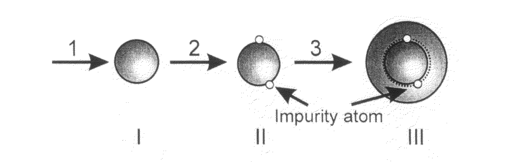
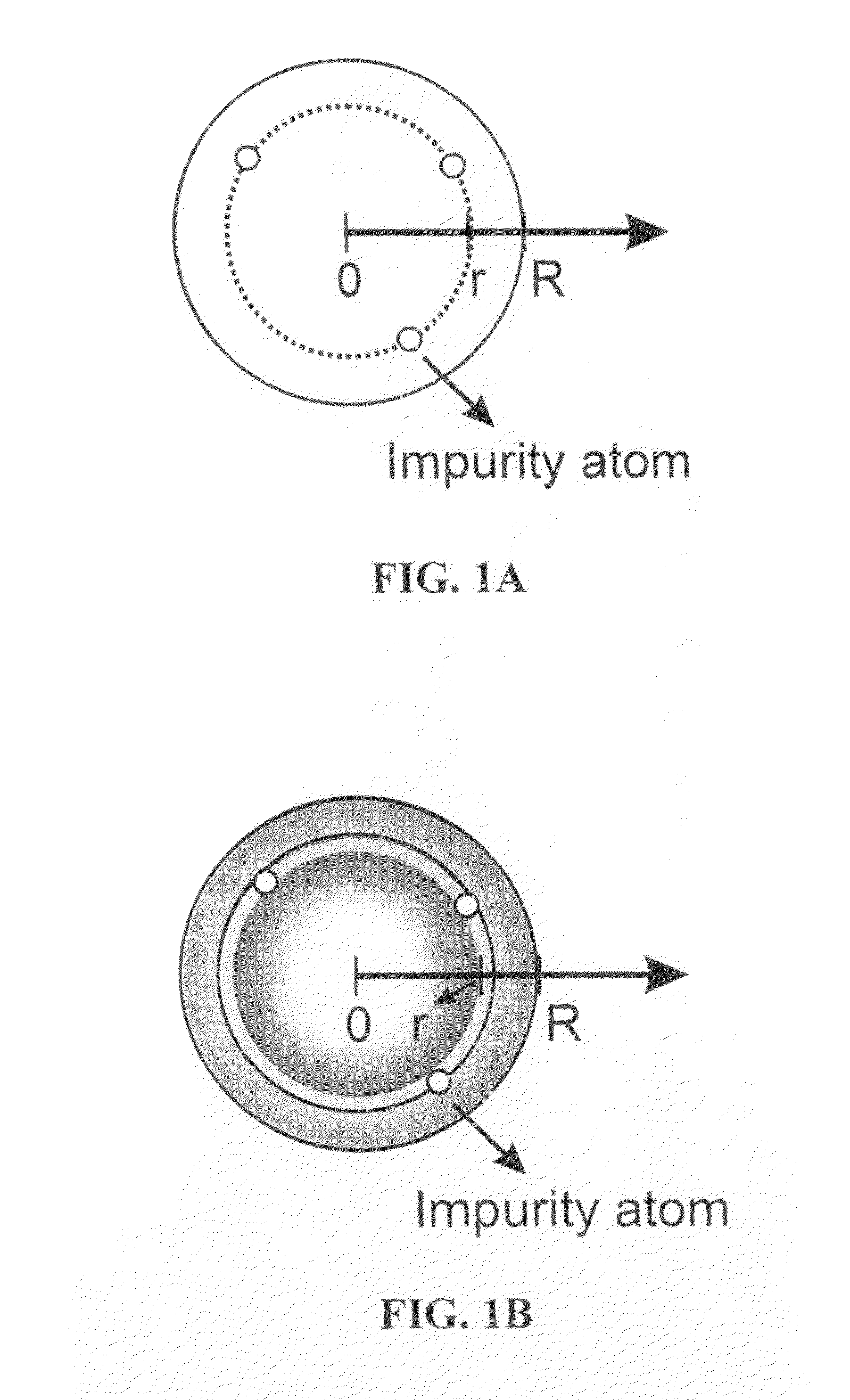
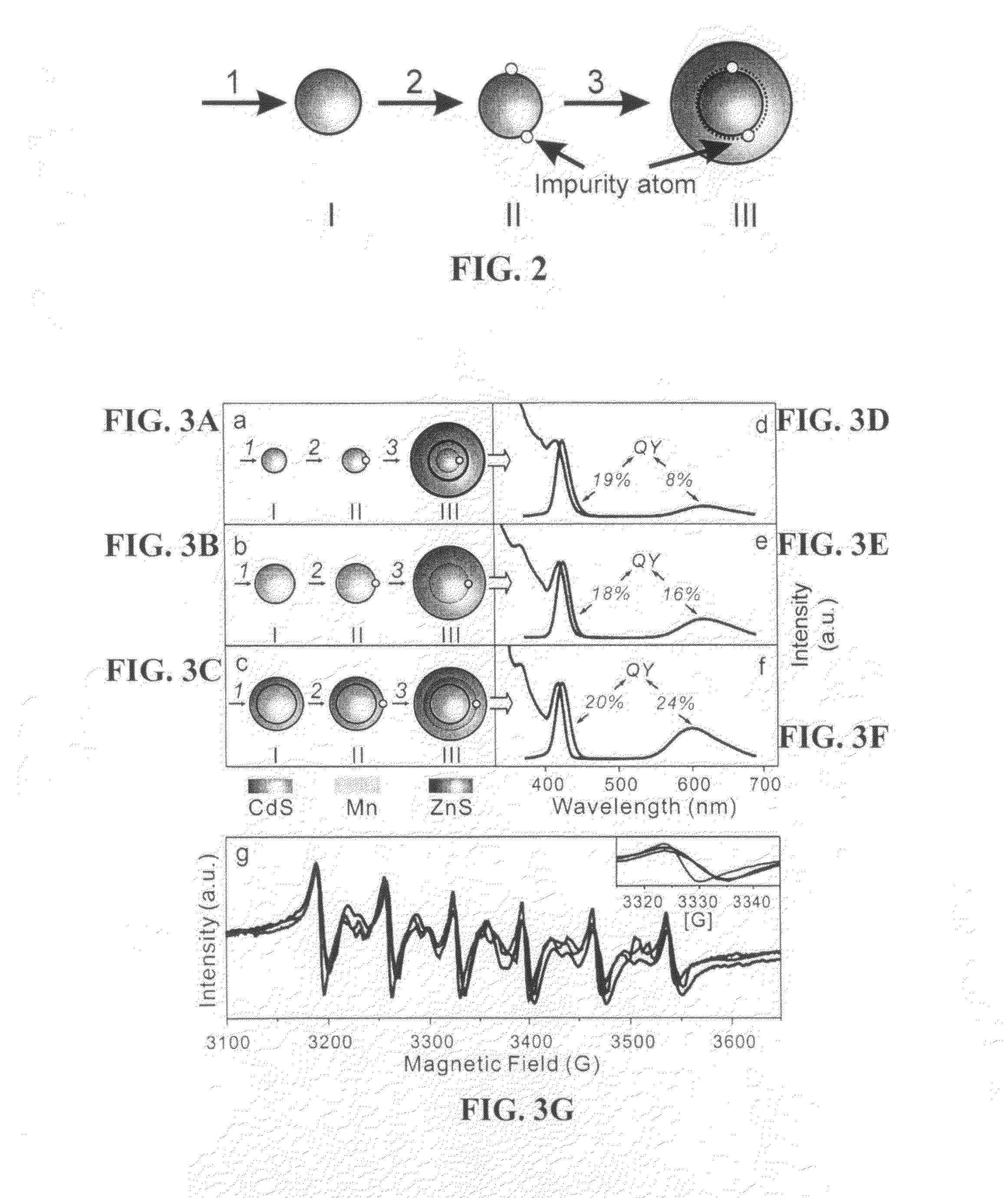
[0060]The three-step synthesis of Mn-doped core / shell nanocrystals begins with the synthesis of starting host particles. Ia and Ib of FIG. 3 show starting host particles of CdS nanocrystals, while Ic of FIG. 3 shows starting host particles of CdS / ZnS core / shell nanocrystals. The starting host particles of CdS / ZnS core / shell nanocrystals can have a thin ZnS shell.
[0061]The synthesis of CdS nanocrystals can be a modification of a literature method.6 In a particular example, cadmium myristate (0.1 mmol) and S (0.05 mmol) were loaded into a three-neck flask with 1-octadecene (ODE, 5 g). In embodiments, the cadmium myristate can be made according to the literature method54. After degassing under vacuum (˜20 mTorr) for 10 min, the vacuum was removed. Then, under argon flow, the temperature was raised to 240° C. The growth was monitored by taking the absorption spectra of aliquots extracted from the reaction solution. When reaching the desired size, the reaction ...
example 2
Dopant Growth
[0063]Once the starting particles are synthesized, the three-step synthesis of Mn-doped core / shell nanocrystals continues with Mn-dopant growth. In this second step, Mn-doping can be achieved by the growth of partial MnS shells onto the starting host particles. Mn-doping levels (i.e., concentration of the dopants) of the nanocrystals can be controlled in this step in direct proportion to the amount of MnS-growth precursors added (e.g., Mn(Ac)2 and S).
[0064]In one example, for Mn-dopant growth using the active precursor Mn(S2CNEt2)2, a hexane solution of starting host particles (CdS or CdS / ZnS) was added into a mixture solution of ODE and oleylamine (3.6 mL of ODE and 1.2 mL of oleylamine), and then hexane was removed under vacuum. Under argon flow, the nanocrystal solution was heated to 220° C., and then an oleylamine solution of the active Mn precursor (Mn(S2CNEt2)2) (0.005 M) was introduced into the hot solution by dropwise addition. After a further 20-min reaction, t...
example 3
Growing the Host Shell
[0069]Finally, the three-step synthesis can be completed by growing the host-shell. Referring to IIIa of FIG. 3, for Mn dopant inside the CdS core of CdS / ZnS core / shell nanocrystals, a hexane solution of Mn-doped CdS nanocrystals was added into a mixture solution of ODE and oleylamine (3.6 mL of ODE and 1.2 mL of oleylamine), and then hexane was removed by vacuum. Under argon flow, the nanocrystal solution was heated to 240° C., and cadmium myristate solution (0.04M in ODE) and S solution (0.04 M in ODE) were alternatively introduced by dropwise addition. The shell growth was monitored by using UV-Vis spectroscopy. After two monolayers (increasing the diameter to 3.8 nm from 2.4 nm), the reaction solution was cooled down to 220° C. Then zinc-stearate solution (0.04M in ODE) and sulfur solution (0.04M in ODE) were alternatively introduced into the hot solution by dropwise addition. When ZnS-shell thickness reached about 1.6 monolayers, the reaction solution was ...
PUM
| Property | Measurement | Unit |
|---|---|---|
| Temperature | aaaaa | aaaaa |
| Reaction temperature | aaaaa | aaaaa |
| Reaction temperature | aaaaa | aaaaa |
Abstract
Description
Claims
Application Information